The whole blog is a correction book at the end. The code is all right and can be simulated normally
1. Introduction to FIFO
2. Synchronous FIFO
A clock is used for reading and writing
Module implementation
Module block diagram
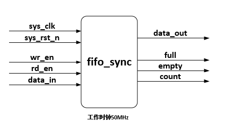
Port introduction:
- sys_clk: 50MHz system clock
- sys_rst_n: System reset, low effective
- wr_en: write enable signal, highly effective
- rd_en: read enable signal, highly effective
- data_in: write data
- data_out: read data
- Full: FIFO full signal, high effective
- Empty: FIFO empty signal, high effective
- count: FIFO data counter. When the read-write pointers are equal, it may be full or empty. It can be judged that it is full according to the value of the counter
Function Description:
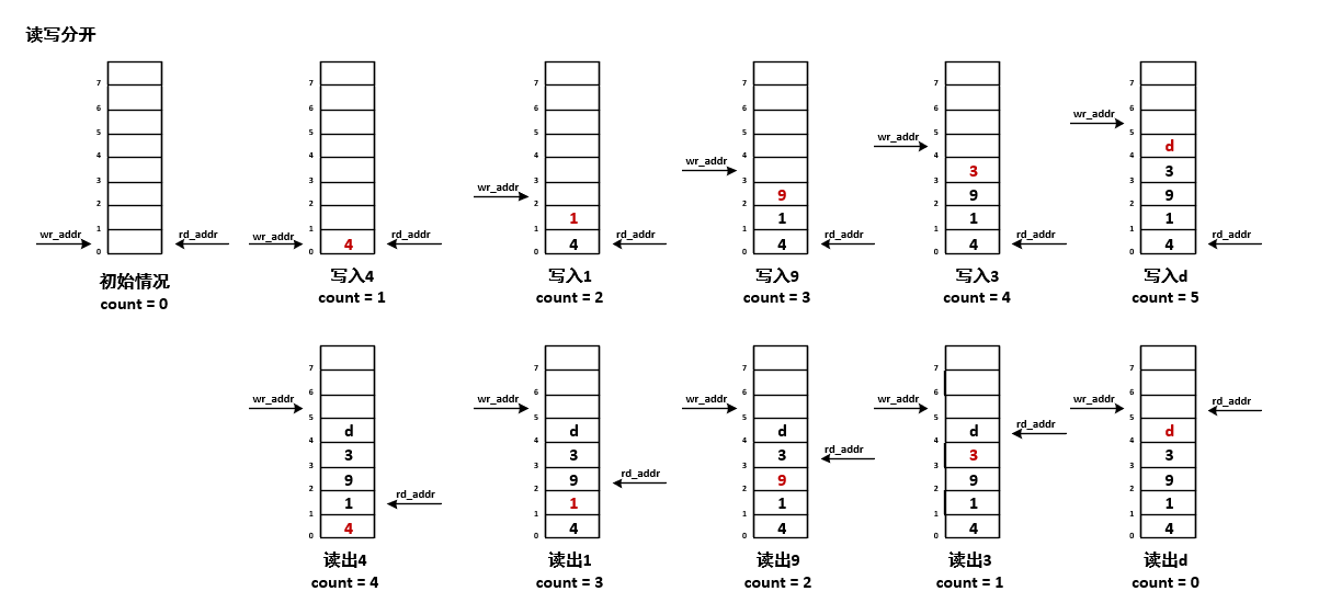
- Take the 4 * 8 size FIFO as an example. The data bit width is 4 bits, the address bit width is 3 bits, [4-1: 0] MEM [{3 {1 'B1}}: 0] / / the addressing range is 0 ~ 3' b111, i.e. 0 ~ 7
- Reset and initialize mem to 0
- Write data, write enable and not full, write data, counter plus 1
- Read data, read enable and not empty, read data, counter minus 1
- Reading and writing are carried out at the same time, only data update is carried out, and the counter remains unchanged
code:
// fifo_4x8, address bit width is 3bit
// Counter working range 0 ~ 7
// When the counter is 8, it proves that it is full. In order for the counter to reach 8, 4bit is required
module fifo_sync
#(
	parameter	data_width	=	4,
				addr_width	=	3
)
(
	input	wire						sys_clk		,
	input	wire						sys_rst_n	,
	input	wire						wr_en		,
	input	wire						rd_en		,
	input	wire	[data_width-1 : 0]	data_in		,

	output	reg		[data_width-1 : 0]	data_out	,
	output	wire						full		,
	output	wire						empty		,
	output	reg		[addr_width   : 0]	count
);
	reg		[addr_width-1 : 0]	wr_addr	;	// Write address, pointing to the next address to write
	reg		[addr_width-1 : 0]	rd_addr	;	// Read address, pointing to the next address to read
	reg		[data_width-1 : 0]	mem	[{addr_width{1'b1}} : 0];	// Declaration memory
	integer	i;		// Used to initialize memory
// mem initialization
	always @ (posedge sys_clk or negedge sys_rst_n)
		if (!sys_rst_n)	begin
			for (i = 0;	i <= {addr_width{1'b1}}; i = i + 1)	// The addressing range is 0~3'b111, i.e. 0 ~ 7
				mem[i]	<=	{data_width{1'b0}};				// The data is initialized to 4'd0000, i.e. 0x0
		end

// Write operation
	always @ (posedge sys_clk or negedge sys_rst_n)
		if (!sys_rst_n)
			wr_addr	<=	0;
		else	if (wr_en && (~full))		// Write enable & memory not full
			begin
				mem[wr_addr]	<=	data_in;
				wr_addr			<=	wr_addr + 1'b1;
			end
		else
			wr_addr	<=	wr_addr;

// Read operation
	always @ (posedge sys_clk or negedge sys_rst_n)
		if (!sys_rst_n)
			begin
				data_out	<=	{data_width-1{1'b0}};		// Output corresponding data bit width 0
				rd_addr		<=	0;
			end
		else	if (rd_en && (~empty))		// Read enable & memory not empty
			begin
				data_out	<=	mem[rd_addr];
				rd_addr		<=	rd_addr + 1'b1;
			end
		else
			begin
				data_out	<=	data_out;
				rd_addr		<=	rd_addr;
			end

// count counter to generate empty full flag
	always @ (posedge sys_clk or negedge sys_rst_n)
		if (!sys_rst_n)
			count	<=	0;
		else	if (wr_en && (~full))	// Write only
			count	<=	count + 1'b1;
		else	if (rd_en && (~empty))	// Read only
			count	<=	count - 1'b1;
		else
			count	<=	count;

	assign	empty	=	(count == 0);
	assign	full	=	(count == {addr_width{1'b1}} + 1'b1);

endmodule
// fifo_4x8
// The data bit width is 4bit and the address bit width is 3bit
module sim_fifo_sync #(
	parameter	data_width	=	4,
				addr_width	=	3
)();
	reg				       		sys_clk		;
	reg			     			sys_rst_n	;
	reg		  				    wr_en		;
	reg			 			     rd_en		;
	reg    	[data_width-1 : 0]	data_in		;

	wire	[data_width-1 : 0]	data_out	;
	wire						full		;
	wire						empty		;
	wire	[addr_width   : 0]	count		;

	integer    i;

	// Instantiate fifo_sync
	fifo_sync
	#(
		.data_width   (data_width)	,
		.addr_width   (addr_width)
	)
	fifo_sync_inst
	(
		.sys_clk	(sys_clk)	,
		.sys_rst_n	(sys_rst_n)	,
		.wr_en		(wr_en)		,
		.rd_en		(rd_en)		,
		.data_in	(data_in)	,

		.data_out	(data_out)	,
		.full		(full)		,
		.empty		(empty)		,
		.count		(count)
	);


	// 50MHz
	localparam	clk_period_50M	=	20;
	always # (clk_period_50M /2 )	sys_clk = ~sys_clk;

	initial	begin
		sys_clk		=	0;
		sys_rst_n	=	0;
		wr_en		=	0;
		rd_en		=	0;
		data_in		=	0;
		#20
		sys_rst_n	=	1;	// Reset end

		wr_en	=	1;		// Write 5 data
		#100
		wr_en	=	0;		// No more
		rd_en	=	1;		// Read 5 data
		#100
		rd_en	=	0;		// No more

		#100
		wr_en	=	1;		// Start writing
		#100
		rd_en	=	1;		// Read while writing
		#100
		wr_en	=	0;
		rd_en	=	0;

		#100
		wr_en	=	1;
		#200
		rd_en	=	1;

	end

	initial    begin
	   for (i = 0; i < 50; i=i+1)
	       #20 data_in = {$random} % 16;
	end

endmodule
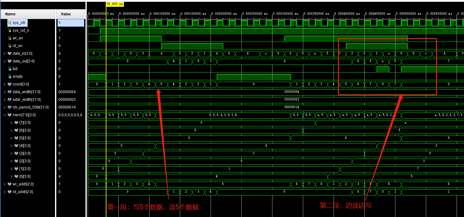
There is no problem when reading and writing are carried out separately. There is a problem when reading and writing are carried out simultaneously
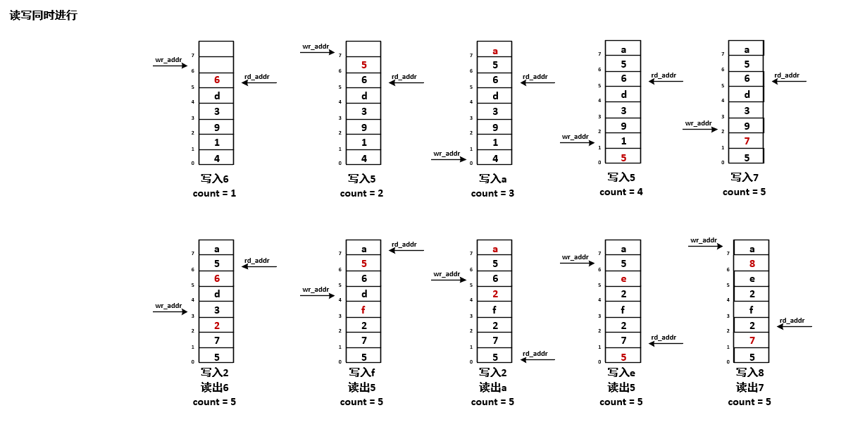
When reading and writing, it is expected that the counter will remain unchanged and only the FIFO data will be updated. Compared with the waveform, it can be seen that the write operation has priority when reading and writing. The if else structure is used in the count module, which has priority and will judge whether to write first
Modify the count counter code
	always @ (posedge sys_clk or negedge sys_rst_n)
		if (!sys_rst_n)
			count	<=	0;
		else	if ((wr_en && (~full)) && (rd_en && (~empty)))	// Read and write operations are performed simultaneously
			count	<=	count;
		else	if (wr_en && (~full))	// Write only
			count	<=	count + 1'b1;
		else	if (rd_en && (~empty))	// Read only
			count	<=	count - 1'b1;
		else
			count	<=	count;
Lower plate verification
- Verification idea:
The working clock of all modules is 50MHz, and the clock of EGO1 system is 100MHz. The frequency division is carried out in the top module.
Firstly, the read-write control key is de chattered, and only one clock cycle high-level flag signal is output when the key is valid;
data_in the 4bit data to be written is determined by the switch;
Read out data_out, write data pointer (address subscript), read data pointer (address subscript) and data number counter count are dynamically displayed with nixie tube
-
Problems encountered in the lower board:
- The initialization operation and write operation are divided into two always blocks: after the reset is invalid, the write data cannot be written in, but in fact, the data_in has been sent, and the read data is always the initialization value. (I don't understand the results after the board verification.). The result of initializing or writing a block of data directly with always is normal
- Initialization and write operations are combined in an always block: the data can be normally written into FIFO by the switch, and the read data is also written later
- After reset, a data will be written by default, which is the value controlled by the current switch. I don't know why it will be written by default, but it does happen
Except that the first data is a little out of control, other conditions are normal writing and normal judgment of empty and full
-
key_filter de dithering module code
module key_filter #( parameter CNT_MAX = 20'd999_999 //Maximum counter count ) ( input wire sys_clk , //System clock 50Mhz input wire sys_rst_n , //Global reset input wire key_in , //Key input signal output reg key_flag //key_ When the flag is 1, it indicates that the key is pressed after de dithering //key_ When the flag is 0, it means that the key is not detected to be pressed ); //reg define reg [19:0] cnt_20ms ; //Counter //cnt_20ms: if the rising edge of the clock detects that the value input by the external key is low, the counter starts counting always@(posedge sys_clk or negedge sys_rst_n) if(sys_rst_n == 1'b0) cnt_20ms <= 20'b0; else if(key_in == 1'b1) cnt_20ms <= 20'b0; else if(cnt_20ms == CNT_MAX && key_in == 1'b0) cnt_20ms <= cnt_20ms; else cnt_20ms <= cnt_20ms + 1'b1; //key_flag: when the count reaches 20ms, the key valid flag bit is generated //And key_flag in 999_ Pull high at 999 to maintain the high level of a clock always@(posedge sys_clk or negedge sys_rst_n) if(sys_rst_n == 1'b0) key_flag <= 1'b0; else if(cnt_20ms == CNT_MAX - 1'b1) key_flag <= 1'b1; else key_flag <= 1'b0; endmodule -
fifo_sync, modify the initialization based on the above code
module fifo_sync #( parameter data_width = 4, addr_width = 3 ) ( input wire sys_clk , input wire sys_rst_n , input wire wr_en , input wire rd_en , input wire [data_width-1 : 0] data_in , output reg [data_width-1 : 0] data_out , output wire full , output wire empty , output reg [addr_width : 0] count , output reg [addr_width-1 : 0] wr_addr , output reg [addr_width-1 : 0] rd_addr ); // reg [addr_width-1 : 0] wr_addr ; // Write address // reg [addr_width-1 : 0] rd_addr ; // Read address reg [data_width-1 : 0] mem [{addr_width{1'b1}} : 0]; // Declaration memory integer i; // Used to initialize memory // mem initialization // always @ (posedge sys_clk or negedge sys_rst_n) // if (!sys_rst_n) begin // for (i = 0; i <= {addr_width{1'b1}}; i = i + 1) // The addressing range is 0~3'b111, i.e. 0 ~ 7 // //mem[i] <= {data_width{1'b1}}; // The data is initialized to 4'd0000, i.e. 0x0 // mem[i] <= 4'd8; // end // Write operation // always @ (posedge sys_clk or negedge sys_rst_n) // if (!sys_rst_n) // wr_addr <= 0; // else if (wr_en && (~full)) // Write enable & memory not full // begin // mem[wr_addr] <= data_in; // wr_addr <= wr_addr + 1'b1; // end // else // wr_addr <= wr_addr; // Initialization and write operations always @ (posedge sys_clk or negedge sys_rst_n) if (!sys_rst_n) begin wr_addr <= 0; for (i = 0; i <= {addr_width{1'b1}}; i = i + 1) // The addressing range is 0~3'b111, i.e. 0 ~ 7 mem[i] <= {data_width{1'b0}}; // The data is initialized to 4'd0000, i.e. 0x0 end else if (wr_en && (~full)) // Write enable & memory not full begin mem[wr_addr] <= data_in; wr_addr <= wr_addr + 1'b1; end else wr_addr <= wr_addr; // Read operation always @ (posedge sys_clk or negedge sys_rst_n) if (!sys_rst_n) begin data_out <= {data_width-1{1'b0}}; // Output corresponding data bit width 0 rd_addr <= 0; end else if (rd_en && (~empty)) // Read enable & memory not empty begin data_out <= mem[rd_addr]; rd_addr <= rd_addr + 1'b1; end else begin data_out <= data_out; rd_addr <= rd_addr; end // count counter to generate empty full flag always @ (posedge sys_clk or negedge sys_rst_n) if (!sys_rst_n) count <= 0; else if ((wr_en && (~full)) && (rd_en && (~empty))) // Read and write operations are performed simultaneously count <= count; else if (wr_en && (~full)) // Write only count <= count + 1'b1; else if (rd_en && (~empty)) // Read only count <= count - 1'b1; else count <= count; // always @ (posedge sys_clk or negedge sys_rst_n) / / there is a small problem when reading and writing are performed at the same time // if (!sys_rst_n) // count <= 0; // else if (wr_en && (~full)) // Write only // count <= count + 1'b1; // else if (rd_en && (~empty)) // Read only // count <= count - 1'b1; // else // count <= count; assign empty = (count == 0) ? 1'b1 : 1'b0; assign full = (count == {addr_width{1'b1}} + 1'b1) ? 1'b1 : 1'b0; endmodule -
Nixie tube dynamic display
Link: Nixie tube dynamic display.module led_dynamic( output reg [7:0] seg, output reg [3:0] an, input wire sys_clk, input wire sys_rst_n, input wire [3:0] in3, in2, in1, in0 ); parameter _0 = ~8'hc0; parameter _1 = ~8'hf9; parameter _2 = ~8'ha4; parameter _3 = ~8'hb0; parameter _4 = ~8'h99; parameter _5 = ~8'h92; parameter _6 = ~8'h82; parameter _7 = ~8'hf8; parameter _8 = ~8'h80; parameter _9 = ~8'h90; parameter _a = ~8'h88; parameter _b = ~8'h83; parameter _c = ~8'hc6; parameter _d = ~8'ha1; parameter _e = ~8'h86; parameter _f = ~8'h8e; parameter _err = ~8'hcf; parameter N = 18; reg [N-1 : 0] regN; reg [3:0] hex_in; always @ (posedge sys_clk or posedge sys_rst_n) begin if (sys_rst_n == 1'b0) begin regN <= 0; end else begin regN <= regN + 1; end end always @ (*) begin case (regN[N-1: N-2]) 2'b00: begin an <= 4'b0001; hex_in <= in0; end 2'b01: begin an <= 4'b0010; hex_in <= in1; end 2'b10: begin an <= 4'b0100; hex_in <= in2; end 2'b11: begin an <= 4'b1000; hex_in <= in3; end default: begin an <= 4'b1111; hex_in <= in3; end endcase end always @ (*) begin case (hex_in) 4'h0: seg <= _0; 4'h1: seg <= _1; 4'h2: seg <= _2; 4'h3: seg <= _3; 4'h4: seg <= _4; 4'h5: seg <= _5; 4'h6: seg <= _6; 4'h7: seg <= _7; 4'h8: seg <= _8; 4'h9: seg <= _9; 4'ha: seg <= _a; 4'hb: seg <= _b; 4'hc: seg <= _c; 4'hd: seg <= _d; 4'he: seg <= _e; 4'hf: seg <= _f; default:seg <= _err; endcase end endmodule -
Top level module
// 4X8, data bit width 4bit, address bit width 3bit // When the EGO1 board is used to lower the board, the system clock is 100MHz. The calling module needs to pay attention to the selection of working clock module top_fifo_sync #( parameter data_width = 4, addr_width = 3 )( input wire sys_clk , // 100MHz input wire sys_rst_n, input wire key_wr, input wire key_rd, input wire [data_width-1 : 0] data_in, output wire [7:0] seg, output wire [3:0] an, output wire full, output wire empty ); wire wr_en ; wire rd_en ; wire [data_width-1 : 0] data_out; wire [addr_width : 0] count ; wire [addr_width-1 : 0] wr_addr ; wire [addr_width-1 : 0] rd_addr ; reg sys_clk_50M; always @ (posedge sys_clk or negedge sys_rst_n) if (!sys_rst_n) sys_clk_50M = 0; else if (sys_clk == 1) sys_clk_50M = ~sys_clk_50M; key_filter key_filter_wr_inst ( .sys_clk (sys_clk_50M), .sys_rst_n (sys_rst_n), .key_in (key_wr), .key_flag (wr_en) ); key_filter key_filter_rd_inst ( .sys_clk (sys_clk_50M), .sys_rst_n (sys_rst_n), .key_in (key_rd), .key_flag (rd_en) ); fifo_sync #( .data_width (data_width) , .addr_width (addr_width) ) fifo_sync_inst ( .sys_clk (sys_clk_50M), .sys_rst_n (sys_rst_n), .wr_en (wr_en), .rd_en (rd_en), .data_in (data_in), .data_out (data_out), .full (full), .empty (empty), .count (count), .wr_addr (wr_addr), .rd_addr (rd_addr) ); led_dynamic led_dynamic_inst ( .sys_clk (sys_clk_50M), .sys_rst_n (sys_rst_n), .in3 (data_out), .in2 (wr_addr), .in1 (rd_addr), .in0 (count), .seg (seg), .an (an) ); endmodule -
Constraint file
set_property -dict {PACKAGE_PIN P17 IOSTANDARD LVCMOS33} [get_ports sys_clk ]
set_property -dict {PACKAGE_PIN P15 IOSTANDARD LVCMOS33} [get_ports sys_rst_n  ]

set_property -dict {PACKAGE_PIN V1  IOSTANDARD LVCMOS33} [get_ports {key_wr}]
set_property -dict {PACKAGE_PIN R11 IOSTANDARD LVCMOS33} [get_ports {key_rd}]

set_property -dict {PACKAGE_PIN R2 IOSTANDARD LVCMOS33} [get_ports {data_in[3]}]
set_property -dict {PACKAGE_PIN M4 IOSTANDARD LVCMOS33} [get_ports {data_in[2]}]
set_property -dict {PACKAGE_PIN N4 IOSTANDARD LVCMOS33} [get_ports {data_in[1]}]
set_property -dict {PACKAGE_PIN R1 IOSTANDARD LVCMOS33} [get_ports {data_in[0]}]

set_property -dict {PACKAGE_PIN G2 IOSTANDARD LVCMOS33} [get_ports {an[3]}]
set_property -dict {PACKAGE_PIN C2 IOSTANDARD LVCMOS33} [get_ports {an[2]}]
set_property -dict {PACKAGE_PIN C1 IOSTANDARD LVCMOS33} [get_ports {an[1]}]
set_property -dict {PACKAGE_PIN H1 IOSTANDARD LVCMOS33} [get_ports {an[0]}]

set_property -dict {PACKAGE_PIN B4 IOSTANDARD LVCMOS33} [get_ports {seg[0]}]
set_property -dict {PACKAGE_PIN A4 IOSTANDARD LVCMOS33} [get_ports {seg[1]}]
set_property -dict {PACKAGE_PIN A3 IOSTANDARD LVCMOS33} [get_ports {seg[2]}]
set_property -dict {PACKAGE_PIN B1 IOSTANDARD LVCMOS33} [get_ports {seg[3]}]
set_property -dict {PACKAGE_PIN A1 IOSTANDARD LVCMOS33} [get_ports {seg[4]}]
set_property -dict {PACKAGE_PIN B3 IOSTANDARD LVCMOS33} [get_ports {seg[5]}]
set_property -dict {PACKAGE_PIN B2 IOSTANDARD LVCMOS33} [get_ports {seg[6]}]
set_property -dict {PACKAGE_PIN D5 IOSTANDARD LVCMOS33} [get_ports {seg[7]}]

set_property -dict {PACKAGE_PIN F6 IOSTANDARD LVCMOS33} [get_ports {full}]
set_property -dict {PACKAGE_PIN G4 IOSTANDARD LVCMOS33} [get_ports {empty}]
3. Asynchronous FIFO
Different clocks are used for reading and writing
Thought supplement
Supplement: $clog2() system function
// Here we still take the 4X8 FIFO as an example

// In the example of synchronous FIFO, given a data bit width of 4bit and an address bit width of 3bit, the addressing range is determined according to the address bit width: [{addr_width {1'b1}: 0]
parameter	data_width	=	4,
parameter	addr_width	=	3
reg		[data_width-1 : 0]	mem	[{addr_width{1'b1}} : 0];
reg		[addr_width-1 : 0]	wr_addr	;	// Write address
reg		[addr_width-1 : 0]	rd_addr	;	// Read address

// If you use the $clog2() system function
// The given data bit width is 4bit, the given data depth is 8, 2 ^ 3 = 8
parameter	data_width	=	4;
parameter	data_depth	=	8;
reg		[data_width-1 : 0]	mem	[data_depth : 0];
reg		[$clog(data_depth)-1 : 0]	wr_addr	;	// Write address 	 [3-1 : 0]
reg		[$clog(data_depth)-1 : 0]	rd_addr	;	// Read address 	 [3-1 : 0]
Here is a supplementary cross clock domain problem
Refer to this blog:
On the problem of cross clock domain transmission (CDC) -- Li Rui Bowen.
FPGA basic knowledge minimalist tutorial (4) asynchronous FIFO from FIFO Design -- Li Rui Bowen.
Supplement:
- fast to slow: the fast clock signal has a short holding time, and the slow clock may not be able to sample. Therefore, the input signal under the fast clock needs to be widened to keep it for a longer time, and then after sampling, a feedback signal is obtained to pull down the widened signal
- slow to fast: the fast clock can sample the slow clock, and the signal of the slow clock will maintain at least one clock cycle under the fast clock
- The synchronous FIFO can be judged to be empty or full by using the counter method, but asynchronous is not allowed, because the read-write pointer is not in a clock domain, and the counter cannot count under such circumstances. It is necessary to synchronize the read-write pointer
The read-write pointer is synchronized to a clock field:
- Full: the read pointer is synchronized to the write clock field
- After reading and writing the registered data in the form of binary code + 1, synchronize the read and write results with the clock pointer, and then convert them to the binary code + 1
- When the read pointer is converted to gray code form and synchronized to the write clock field, the read and write data may be in progress, and the read and write pointers may also be increasing. When the synchronized read and write pointers are equal, the actual read pointer may have changed. In this case, there is still space not full (read)
- Null determination: the write pointer is synchronized to the read clock field
- After writing data, write pointer + 1, convert the result value into gray code property, register one beat, and then use the two-stage synchronization of reading clock to convert the synchronized signal into binary code, and register one beat for comparison with the reading pointer
- When the write pointer is converted to gray code form and synchronized to the write clock field, the read-write data may be in progress, and the read-write pointer may also be increasing. When the synchronized read-write pointers are equal, the actual write town may have changed, which is equivalent to writing more
Application of gray code conversion:
-
Gray code is a kind of security code, because the adjacent gray code has only one bit, which is different from binary. Binary generally has many adjacent bits. In the transmission of gray code, because there is only one adjacent bit different, its bit error rate is much lower than that of binary code.
In synchronization, the probability of metastable state is also lower than that of binary.// Binary to gray code gray = binary ^ (binary >>> 1)
-
When gray code is converted between any two adjacent numbers, only one bit changes, so it effectively avoids the unstable state of the register from one value to the next value. And because there is only one bit difference between the maximum number and the minimum number in gray code, it is usually called cyclic binary code or reflective binary code.
-
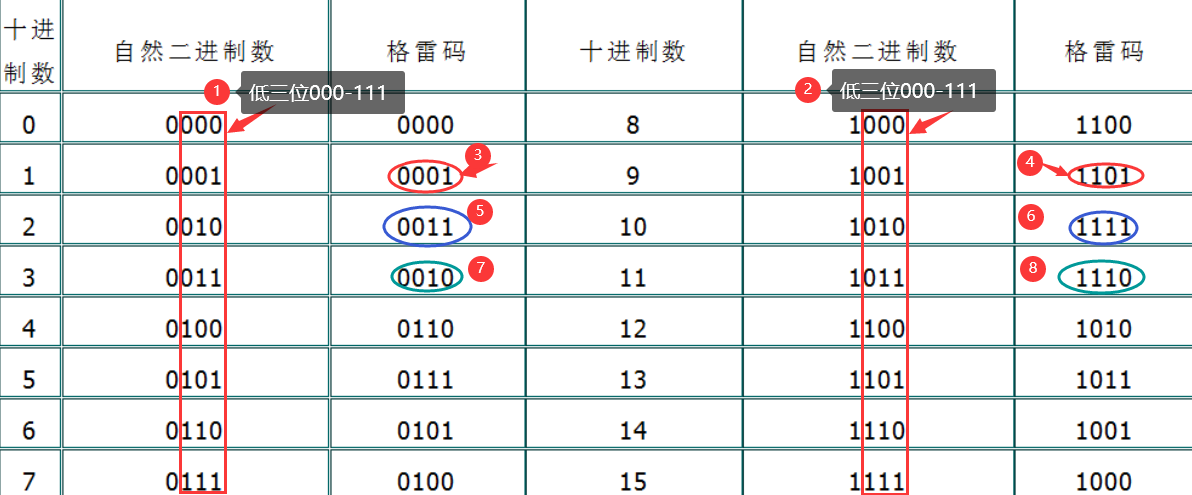
Here, take the FIFO with depth of 8 as an example. The actual address width is [2:0], and 3bit is enough. However, in the application, add 1 bit to the width and define bit [3:0].
- Observe the binary number. One more bit of width has no effect on the pointer. When the address is 3bit, add 1 after all 1 to become all 0; When the address is 4bit, the lower three bits are all 1, and then add 1 to become all 0. All of them are in 3b'111 ~ 3'b000 cycle, and there will be no overflow and cross-border.
- Observe the gray code and look across a line. For a pair of code values with a size difference of 8, the upper two bits are opposite, and the other bits are equal. For example, 5 and 6 correspond to gray codes 4'd0111 and 4'd1011.
- For the extra bit, 0 ~ 7 and 8 ~ 15 can be divided into two groups (originally only 0 ~ 7 address position), and the empty and full can be judged by the characteristics of gray code.
- Gray code is empty if all parts are equal. The read and write pointers are equal, and in a group, it is proved that the read pointer catches up with the write pointer and reads null
- The gray code is full if the two high bits are opposite and the other bits are equal. The read and write pointers are equal. They are in two groups respectively, which proves that the write pointer catches up with the read pointer and is full
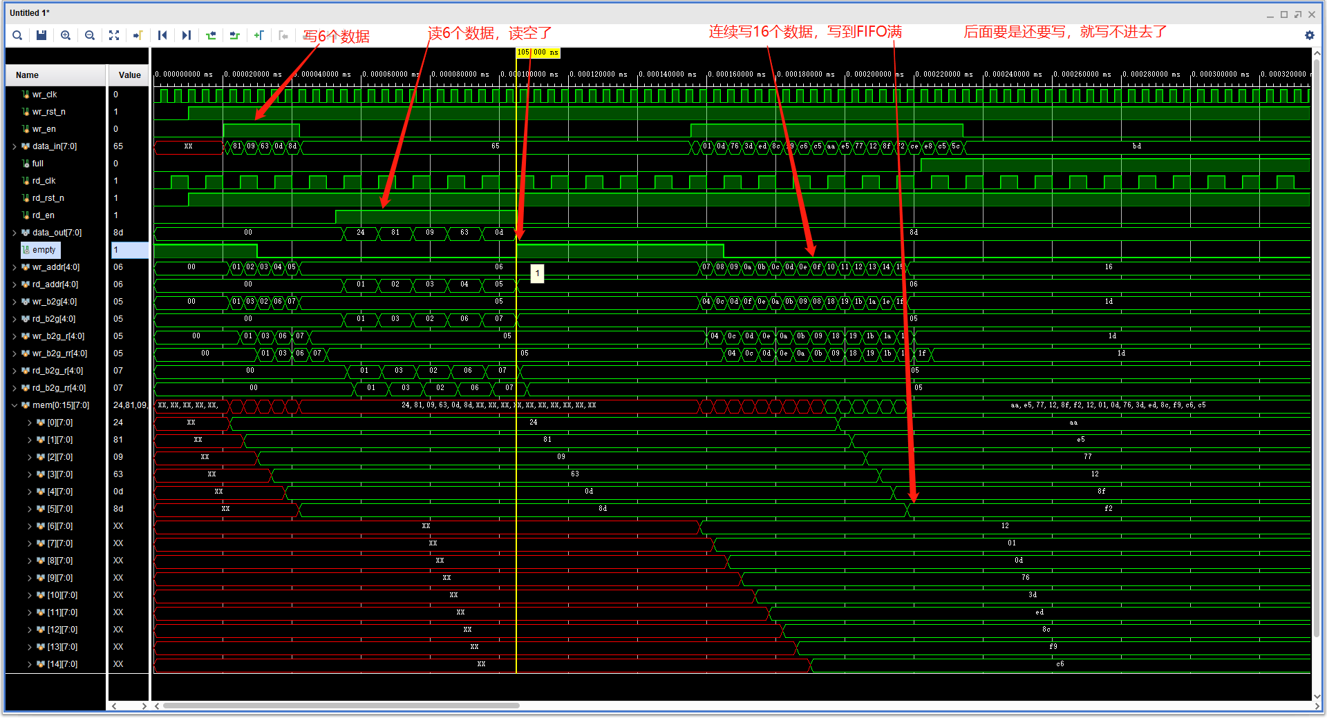
Hasty code implementation, as well as the simulation test with hard results
full and empty signals are realized by sequential logic and combinational logic respectively. Finally, the problem analysis is mentioned
// fifo_8x32
module fifo_async
#(
parameter data_width = 8,
data_depth = 32
)
(
input wire wr_clk ,
input wire wr_rst_n,
input wire wr_en ,
input wire [data_width-1 : 0] data_in ,
output reg full ,
input wire rd_clk ,
input wire rd_rst_n,
input wire rd_en ,
output reg [data_width-1 : 0] data_out,
output wire empty
);
// Define FIFO 8x32
reg [data_width-1 : 0] mem [0 : data_depth-1];
// Definition register
reg [$clog2(data_depth) : 0] wr_addr = 0 ; // Write pointer [5:0]
reg [$clog2(data_depth) : 0] rd_addr = 0 ; // Read pointer [5:0]
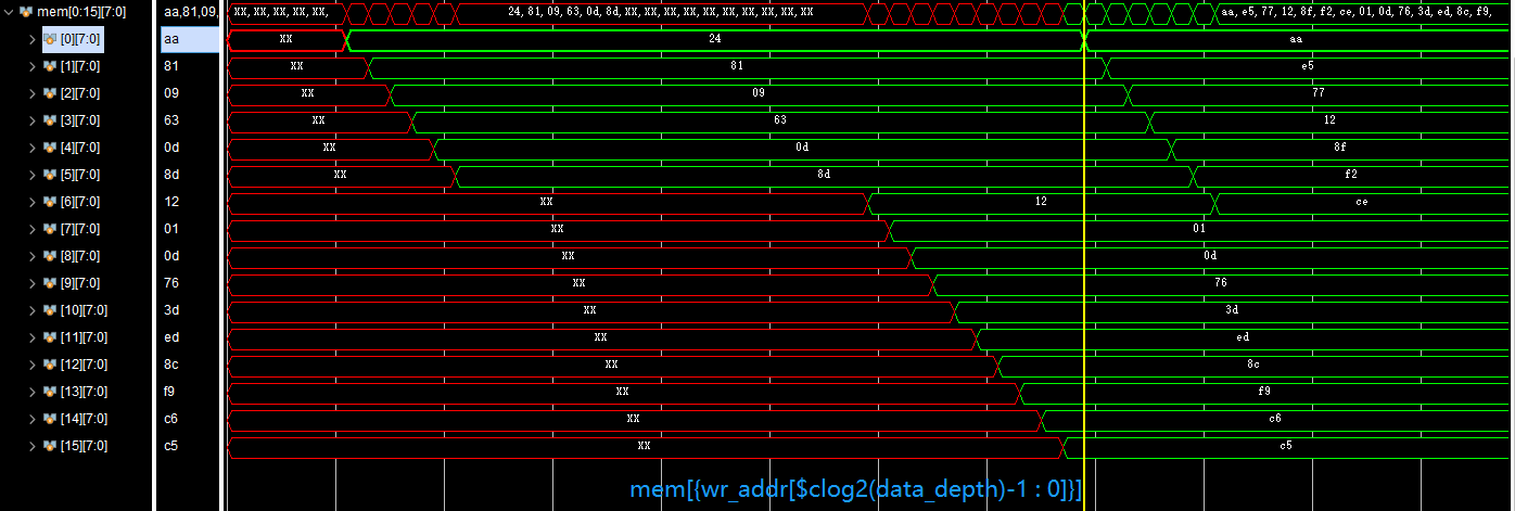
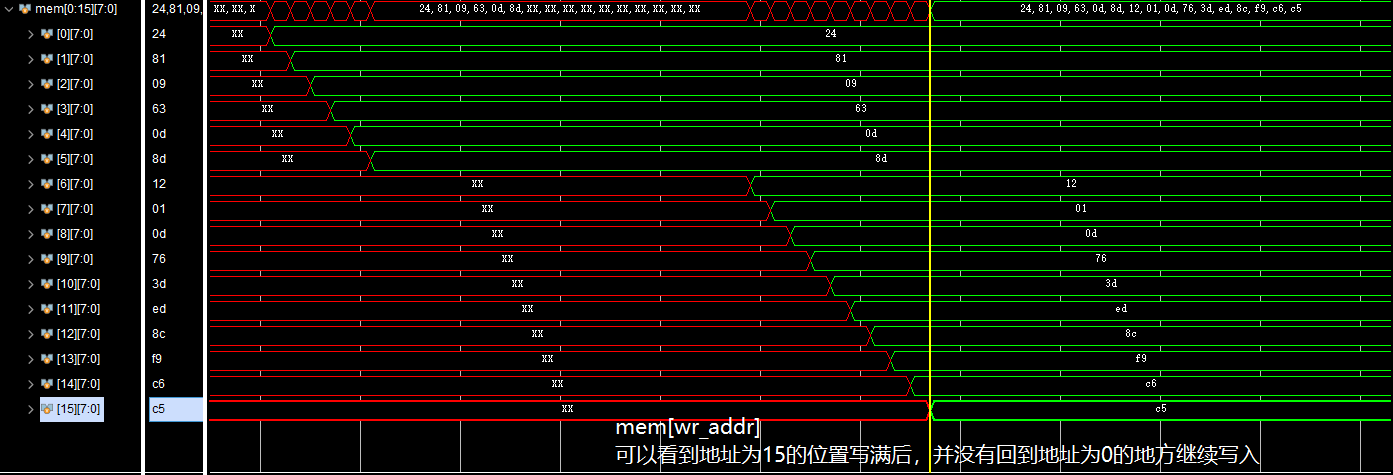
// Compare MEM [{wr_addr [$clog2 (data_depth) - 1: 0]}] and mem[wr_addr]. The following problem analysis talks about the differences between the two addressing modes
// wire [data_width-1 : 0] s1;
// wire [data_width-1 : 0] s2;
// assign s1 = mem[{wr_addr[$clog2(data_depth)-1 : 0]}]; // FIFO data can be read out correctly
// assign s2 = mem[wr_addr]; // The readout is in the high resistance state, which proves that there is no data written in this position
// Write operation
always @ (posedge wr_clk or negedge wr_rst_n)
if (!wr_rst_n)
wr_addr <= 0;
// else if (wr_en && (~full))
else if (wr_en && ~((~rd_b2g_rr[$clog2(data_depth) : $clog2(data_depth)-1] == wr_b2g[$clog2(data_depth) : $clog2(data_depth)-1])
&& (rd_b2g_rr[$clog2(data_depth)-2 : 0] == wr_b2g[$clog2(data_depth)-2 : 0])))
begin
wr_addr <= wr_addr + 1'b1;
// Here because wr_addr defines one bit wider than the actual bit. Here, the address except the highest bit is extracted
// Take the depth of 16 as an example, mem[0:15][7:0]. For example, after the first group of data is written, go back and write new data for the first address. At this time, wr_addr =5'b 1_0000, direct MEM [wr_addr] < = Data_ In, the data is actually not written to the position you want to write
mem[{wr_addr[$clog2(data_depth)-1 : 0]}] <= data_in;
// mem[wr_addr] <= data_in;
end
else
wr_addr <= wr_addr;
// Read operation
always @ (posedge rd_clk or negedge rd_rst_n)
if (!rd_rst_n)
begin
rd_addr <= 0;
data_out <= 0;
end
else if (rd_en && (~empty))
begin
rd_addr <= rd_addr + 1'b1;
data_out <= mem[rd_addr];
end
else
begin
rd_addr <= rd_addr;
data_out <= data_out;
end
wire [$clog2(data_depth) : 0] wr_b2g;
wire [$clog2(data_depth) : 0] rd_b2g;
// Read / write pointer binary to gray code Combined logic is adopted to reduce the number of shots
assign wr_b2g = wr_addr ^ (wr_addr >> 1);
assign rd_b2g = rd_addr ^ (rd_addr >> 1);
// Two level register for beat Here, two registers are directly used for synchronization. Attention should be paid to the CDC problem
reg [$clog2(data_depth) : 0] wr_b2g_r ;
reg [$clog2(data_depth) : 0] wr_b2g_rr ;
reg [$clog2(data_depth) : 0] rd_b2g_r ;
reg [$clog2(data_depth) : 0] rd_b2g_rr ;
// The write pointer is synchronized to the read clock field for null judgment
// always @ (posedge rd_clk or negedge rd_rst_n)
always @ (rd_clk)
if (!rd_rst_n)
begin
wr_b2g_r <= 0;
wr_b2g_rr <= 0;
end
else
begin
wr_b2g_r <= wr_b2g;
wr_b2g_rr <= wr_b2g_r;
end
// always @ (posedge rd_clk or negedge rd_rst_n) // Sequential logic
// if (!rd_rst_n)
// empty <= 0;
// //All bits are equal, null
// else if (wr_b2g_rr == rd_b2g)
// empty <= 1;
// else
// empty <= 0;
assign empty = (wr_b2g_rr == rd_b2g) ? 1 : 0; // combinational logic
// The read pointer is synchronized to the write clock field for full judgment
// always @ (posedge wr_clk or negedge wr_rst_n)
always @ (wr_clk)
if (!wr_rst_n)
begin
rd_b2g_r <= 0;
rd_b2g_rr <= 0;
end
else
begin
rd_b2g_r <= rd_b2g;
rd_b2g_rr <= rd_b2g_r;
end
always @ (posedge wr_clk or negedge wr_rst_n)
if (!wr_rst_n)
full <= 0;
// The higher two digits are opposite, the other digits are equal, and the judgment is full
else if ( (~rd_b2g_rr[$clog2(data_depth) : $clog2(data_depth)-1] == wr_b2g[$clog2(data_depth) : $clog2(data_depth)-1])
&& (rd_b2g_rr[$clog2(data_depth)-2 : 0] == wr_b2g[$clog2(data_depth)-2 : 0]) )
full <= 1;
else
full <= 0;
endmodule
`define	 clk_period_wr 50
`define	 clk_period_rd 20

module sim_fifo_async ();
	parameter		data_width = 8;
	parameter		data_depth = 16;

    reg							wr_clk	;
    reg							wr_rst_n;
    reg							wr_en	;
    reg		[data_width-1 : 0]	data_in	;
    wire						full	;

    reg							rd_clk	;
    reg							rd_rst_n;
    reg							rd_en	;
    wire	[data_width-1 : 0]	data_out;
    wire						empty	;

    fifo_async #(
		.data_width	(data_width),
		.data_depth	(data_depth)
		)
	fifo_async_inst (
		.wr_clk			(wr_clk),
		.wr_rst_n		(wr_rst_n),
		.wr_en			(wr_en),
		.data_in		(data_in),
		.full			(full),

		.rd_clk			(rd_clk),
		.rd_rst_n		(rd_rst_n),
		.rd_en			(rd_en),
		.data_out		(data_out),
		.empty			(empty)
	);

	//always #(`clk_period_wr/2) wr_clk = ~wr_clk;
	//always #(`clk_period_rd/2) rd_clk = ~rd_clk;
	always #(4/2) wr_clk = ~wr_clk;
	always #(10/2) rd_clk = ~rd_clk;

	initial	begin
		wr_clk	=	0;
		rd_clk	=	0;
		wr_rst_n	=	0;
		rd_rst_n	=	0;
		wr_en	=	0;
		rd_en	=	0;
		#10
		wr_rst_n	=	1;
		rd_rst_n	=	1;

		// Start writing, 6 data
		#10
		wr_en = #(0.2) 1'b1;
		data_in	=	#(0.2) $random;
		repeat(5) begin
            @(posedge wr_clk);
                data_in = #(0.2) $random;
        end

        @(posedge wr_clk);
        wr_en = #(0.2) 1'b0;
        data_in = #(0.2) $random;

        // Start reading, read empty
        #10
        rd_en = #(0.2) 1'b1;
        repeat(5) begin
            @(posedge rd_clk);
        end

        @(posedge rd_clk);
        rd_en = #(0.2) 1'b0;


        // When the FIFO is full, you will see the full flag signal
        #50
        wr_en = #(0.2) 1'b1;
        data_in = #(0.2) $random;
        repeat(19) begin
            @(posedge wr_clk);
                data_in = #(0.2) $random;
        end
        @(posedge wr_clk);
        wr_en = #(0.2) 1'b0;
        data_in = #(0.2) $random;

	end

endmodule
Problems encountered and one-sided analysis:
-
As for whether the empty signal can work normally, the excitation signal given by the simulation must pay attention to writing a group of data in the same way, but because the signal change time is different, it will affect the state of the relevant register and the empty and full signal.
-
About wr_addr defines the impact of one more bit. As mentioned above, it has no impact, but it still has a little impact on the addressing of mem
-
There is no good solution to the cross clock domain problem of read-write flag. The results can be obtained normally after crossing the clock domain, which is a little reluctant. During the test, many group cycles have been modified, from T(wr_clk) = 4, T(rd_clk) = 10, to T(wr_clk) = 300, T(rd_clk) = 20, which can read and write correctly and generate the correct empty and full flag
This blog is finished and has a new goal. Reorganize the cross clock domain
Single bit data as an example
- slow2fast, the fast clock can sample the slow clock, and the signal of the slow clock will maintain at least one clock cycle under the fast clock
- fast2slow: the signal holding time under the fast clock is short, and the slow clock may not be sampled. The method of two beats of the register used in the code is not applicable, and other methods are needed to solve it, such as widening the input signal
-
For request control of read and write operations, take writing data as an example,
// Write operation
	always @ (posedge wr_clk or negedge wr_rst_n)
		if (!wr_rst_n)
			wr_addr	<=	0;
		else	if (wr_en && (~full))
			begin
				wr_addr			<=	wr_addr + 1'b1;
				mem[{wr_addr[$clog2(data_depth)-1 : 0]}]	<=	data_in;
			end
		else
			wr_addr	<=	wr_addr;
// Full sentence
	always @ (posedge wr_clk or negedge wr_rst_n)
	if (!wr_rst_n)
		full	<=	0;
	// The higher two digits are opposite, the other digits are equal, and the judgment is full
	else	if ( (~rd_b2g_rr[$clog2(data_depth) : $clog2(data_depth)-1] == wr_b2g[$clog2(data_depth) : $clog2(data_depth)-1])
				&& (rd_b2g_rr[$clog2(data_depth)-2 : 0] == wr_b2g[$clog2(data_depth)-2 : 0]) )
		full	<=	1;
	else
		full	<=	0;
Simulation results: I've been writing data for a long time. It's true that the full signal also outputs a high level, but it only outputs for a short period of time.
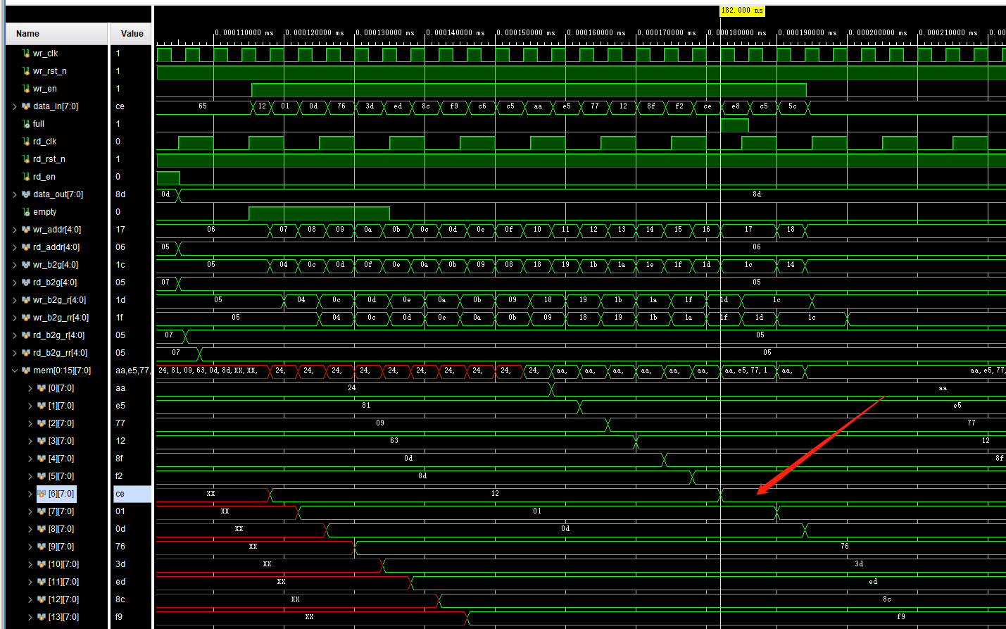
The full signal is obtained using sequential logic. If (wr_en & & (~ full)) is used as the control condition, wr_ EN is stimulated in real time, while full is compared with a late shot. They match briefly (the position of the red arrow), and then miss it
The control conditions are modified as follows:,else if (wr_en && ~((~rd_b2g_rr[$clog2(data_depth) : $clog2(data_depth)-1] == wr_b2g[$clog2(data_depth) : $clog2(data_depth)-1]) && (rd_b2g_rr[$clog2(data_depth)-2 : 0] == wr_b2g[$clog2(data_depth)-2 : 0]))) begin wr_addr <= wr_addr + 1'b1; mem[{wr_addr[$clog2(data_depth)-1 : 0]}] <= data_in; end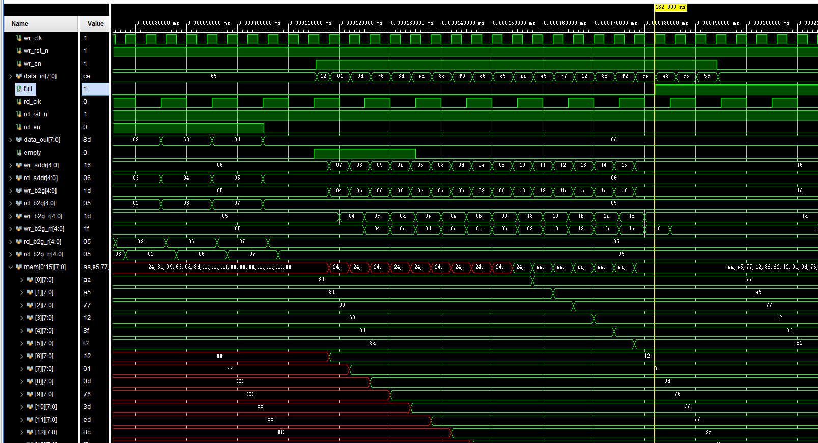
Guess: if the full signal is of wire type and assigned with the assign statement, it is real-time. It can be if ((wr_en & & (~ full)). Let me try to use the empty signal in this way
I've tried, and it's right
Review question 1. The empty signal does not work normally, and question 4 is the same reason. It's OK to modify it.
summary
- Combinatorial logic is also to assist sequential logic. We should pay attention to the synchronization of beats
- Other people's blogs are technology sharing. My blog is like an error correction book. When I encounter various problems, I patch and modify them
Finally finished
4.29 to 5.18
It's annoying