catalogue
1. Theoretical introduction
uart: Universal Asynchronous Receiver / transmitter, which is a serial transceiver. Since there is no clock, both parties need to agree on the transmission rate, start and stop. In order to ensure the reliable transmission of data, check bits need to be used. uart protocol is shown in the figure below
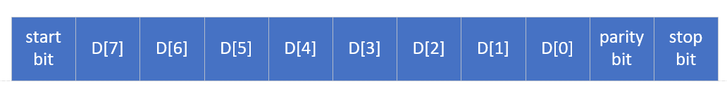
Figure 1 uart protocol
When the protocol does not start transmission, the level on the physical layer path is high, and the start bit pulls the level down, which means that the transmission starts. Here, the large end transmission mode is used, that is, the high byte data is transmitted first, and after the 8-bit data bit transmission is completed, Parity bits are used for verification (an error checking method, but error correction is not allowed), and finally 1 bit / 1.5 bits / 2 stop bits are transmitted.
In the past, I always thought that the communication protocol should have a unified structure standard. Here I dare to define it like this. If there is a problem, correct it at any time. Here I define the physical layer and link layer first:
Physical layer: the main task is to determine some characteristics related to the interface of transmission media
Mechanical characteristics: indicate the shape and size of the connector used for the interface, the number and arrangement of pins, fixing and locking devices, etc.
Electrical characteristics: indicate the voltage range, impedance matching, transmission rate, etc. on each line of the interface cable.
Functional characteristics: indicate the function allocation and exact definition of each signal line on the physical interface.
Process characteristics: indicate the sequence of various possible events for different functions (understood as establishing physical connection, maintaining and exchanging information)
Data link layer: reliable transmission of data from the physical layer in the future. How to transmit reliably is the content specified in the protocol, which is transmitted in frames.
The uart protocol understood here is a protocol that does not define the physical layer but only the protocol layer. Therefore, we can transmit through single ended line, RS232, RS485 or other interfaces. Different interfaces will cause differences in transmission distance and rate. We can freely select interfaces according to our own needs.
2. Architecture design
Before writing the code, it is necessary to build the module block diagram. First analyze which modules are required for uart. This is an asynchronous full duplex protocol. Therefore, a transmitting module and a receiving module are required to realize baud rate generation and data transceiver in their respective modules. The modules and their signals are as follows:
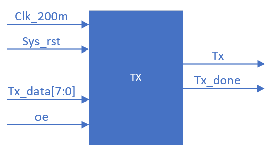
Figure 2. Transmission module
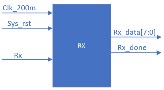
Figure 3. Receiving module
After the top-level module block diagram division is completed, each module needs to be analyzed. The internal main circuit schematic diagram of the transmitting module is shown in Figure 4, and the internal main circuit block diagram of the receiving module is shown in Figure 5. Start to write the program according to the designed circuit block diagram.
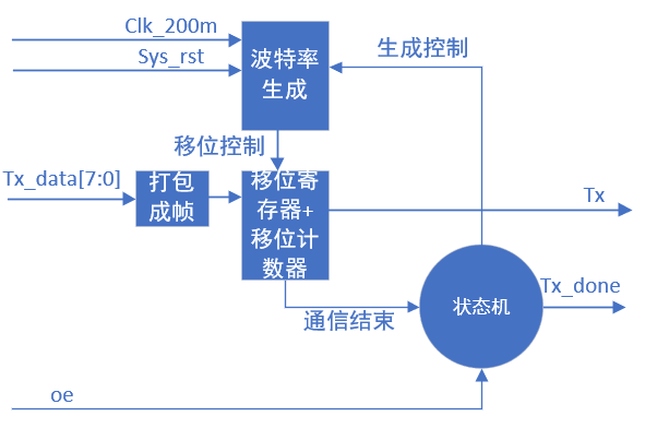
Fig. 4 internal main circuit diagram of transmission module
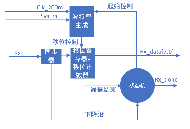
Fig. 5 main internal circuit diagram of receiving module
3. Code design
1, Send module code
/***************************************
#
#			Filename:tx.v
#
#			Developer:annotater
#			Description:---
#			CreatTime:2021-08-09 23:00:12
#
***************************************/
module tx(
input clk_200m,
input sys_rst,
input[7:0] tx_data,
input oe,
output tx,
output reg tx_done
);

localparam BAUD = 115200;
localparam DIV_NUM = 200000000/BAUD;
localparam IDLE = 3'b001;
localparam PRE	= 3'b010;
localparam SEND = 3'b100;

reg[2:0] cstate,nstate;//Define current state and secondary state
reg[11:0] cout;//Baud rate division count
reg[3:0] shift_num;//Shift times
reg[10:0] tx_data_pre;//A frame of data to be sent
wire baud_pdg;//Rising edge of baud rate
wire baud_ndg;//Falling edge of baud rate

//buad generater
always@(posedge clk_200m or posedge sys_rst)begin
	if(sys_rst)begin
		cout <= 12'b0;
	end
	else if(cout == DIV_NUM-1'b1)begin
		cout <= 12'b0;
	end
	else if(cstate == SEND)begin
		cout <= cout + 1'b1;
	end
end
assign baud_pdg = (cout == DIV_NUM >> 1'b1 )?1'b1:1'b0;
assign baud_ndg = (cout == DIV_NUM -  1'b1 )?1'b1:1'b0;

//shift
always@(posedge clk_200m or posedge sys_rst)begin
	if(sys_rst)begin
		tx_data_pre[10:0] <= 11'b1111_1111_11;
		shift_num <= 4'd0;
	end
	else if(cstate == PRE)begin
		tx_data_pre[10:0] <= {1'b0,tx_data,(^tx_data),1'b1};
	end
    else if(shift_num == 4'd10 && baud_ndg)begin
        tx_data_pre[10:0] <= 11'b1111_1111_11;
        shift_num <= 4'd0;
    end
	else if(baud_ndg)begin
		tx_data_pre[10:0] <= {tx_data_pre[9:0],1'b1};
		shift_num <= shift_num + 1'b1;
	end

end

//state machine
always@(posedge clk_200m or posedge sys_rst)begin
	if(sys_rst)begin
		cstate <= IDLE;
	end
	else begin
		cstate <= nstate;
	end
end
always@(*)begin
	case(cstate)//synthesis full_case
		IDLE:nstate = (oe)?PRE:IDLE;
		PRE :nstate = SEND;
		SEND:nstate = (shift_num == 4'd10 && baud_ndg)?IDLE:SEND;
	endcase
end
always@(posedge clk_200m or posedge sys_rst)begin
	if(sys_rst)begin
		tx_done <= 1'b0;
	end
	else begin
		case(cstate)
			IDLE:tx_done <= 1'b0;
			PRE :;
			SEND:begin
				if(shift_num == 4'd10 && baud_ndg)
					tx_done <= 1'b1;
				else
					tx_done <= 1'b0;
			end
		endcase
	end
end
assign tx = (cstate == SEND)?tx_data_pre[10]:1'b1;
endmodule
2, Receiving code design
/***************************************
#
#			Filename:rx.v
#
#			Developer:annotater
#			Description:---
#			CreatTime:2021-08-10 17:44:59
#
***************************************/
module rx(
input clk_200m,
input sys_rst,
input rx,

output reg[7:0] rx_data,
output reg rx_done
);

localparam BAUD = 115200;
localparam DIV_NUM = 200000000/BAUD;
localparam IDLE = 2'b01;
localparam RECE = 2'b10;

reg[1:0] cstate,nstate;//Define current state and secondary state
reg[11:0] cout;//Baud rate division count
reg[3:0] shift_num;//Shift times
reg[10:0] rx_data_rec;//Receive a frame of data
reg[1:0] rx_d;//Synchronizer is used to eliminate metastable state and detect falling edge
wire baud_pdg;//Rising edge of baud rate
wire baud_ndg;//Falling edge of baud rate
wire rx_ndg;//Falling edge of start bit
wire rx_error;//Start bit receive error
//buad generater
always@(posedge clk_200m or posedge sys_rst)begin
	if(sys_rst)begin
		cout <= 12'b0;
	end
	else if(cout == DIV_NUM - 1'b1 )begin
		cout <= 12'b0;
	end
	else if(cstate == RECE)begin
		cout <= cout + 1'b1;
	end
end
assign baud_pdg = (cout == DIV_NUM >> 1'b1 )?1'b1:1'b0;
assign baud_ndg = (cout == DIV_NUM -  1'b1 )?1'b1:1'b0;

//Synchronizer
always@(posedge clk_200m or posedge sys_rst)begin
	if(sys_rst)begin
		rx_d <= 2'b11;
	end
	else begin
		rx_d <= {rx_d[0],rx};
	end
end
assign rx_ndg = rx_d[1] & ~(rx_d[0]);

assign rx_error = (baud_pdg&&(cstate == RECE)&&rx&&(shift_num == 4'b0000));//Judge whether the start bit detects an error

//shift
always@(posedge clk_200m or posedge sys_rst)begin
	if(sys_rst)begin
		rx_data_rec[10:0] <= 11'b0;
	end
	else if(baud_pdg)begin
		rx_data_rec[10:0] <= {rx_data_rec[9:0],rx};
	end
end
always@(posedge clk_200m or posedge sys_rst)begin
    if(sys_rst)
        shift_num <= 0;
    else if(shift_num == 10 && baud_ndg)
        shift_num <= 0;
    else if(baud_ndg)
        shift_num <= shift_num + 1;
end
always@(posedge clk_200m or posedge sys_rst)begin
    if(sys_rst)
        rx_data <= 8'd0;
    else if(rx_done && ~(^rx_data_rec[9:1]))
        rx_data <= rx_data_rec[9:2];
end

//state machine

always@(posedge clk_200m or posedge sys_rst)begin
	if(sys_rst)begin
		cstate <= IDLE;
	end
	else begin
		cstate <= nstate;
	end
end
always@(*)begin
	case(cstate)//synthesis full_case
		IDLE:nstate = (rx_ndg)?RECE:IDLE;
		RECE:nstate = (shift_num == 4'd10 && baud_ndg || rx_error)?IDLE:RECE;
	endcase
end
always@(posedge clk_200m or posedge sys_rst)begin
	if(sys_rst)begin
		rx_done <= 1'b0;
	end
	else begin
		case(cstate)
			IDLE:rx_done <= 1'b0;
			RECE:begin
				if(shift_num == 4'd10 && baud_ndg)
					rx_done <= 1'b1;
				else
					rx_done <= 1'b0;
			end
		endcase
	end
end
endmodule
3, Top level module design
Attention should be paid to avoid glue logic in the top-level module.
/***************************************
#
#			Filename:uart_top.v
#
#			Developer:annotater
#			Description:---
#			CreatTime:2021-08-10 18:15:58
#
***************************************/
module uart_top(
input clk_200m,
input sys_rst,

input rx,
input [7:0] tx_data,
input oe,

output [7:0] rx_data,
output tx,
output rx_done,
output tx_done
);


rx U_RX(
    .clk_200m  ( clk_200m  ), //i
    .sys_rst   ( sys_rst   ), //i
    .rx        ( rx        ), //i
    .rx_data   ( rx_data   ), //o
    .rx_done   ( rx_done   )  //o
);


tx U_TX(
    .clk_200m  ( clk_200m  ), //i
    .sys_rst   ( sys_rst   ), //i
    .tx_data   ( tx_data   ), //i
    .oe        ( oe        ), //i
    .tx        ( tx        ), //o
    .tx_done   ( tx_done   )  //o
);

endmodule
IV. test code
`timescale 1ns / 1ps
//
// Company:
// Engineer:
//
// Create Date: 2021/08/10 18:21:32
// Design Name:
// Module Name: tb_uart_top
// Project Name:
// Target Devices:
// Tool Versions:
// Description:
//
// Dependencies:
//
// Revision:
// Revision 0.01 - File Created
// Additional Comments:
//
//
module tb_uart_top();
reg      clk_200m    ;
reg      sys_rst     ;
reg      rx          ;
reg[7:0] tx_data     ;
reg      oe          ;
wire[7:0] rx_data     ;
wire      tx          ;
wire      rx_done     ;
wire      tx_done     ;
initial begin
clk_200m = 0;
sys_rst = 1;
rx = 0;
tx_data= 0;
oe = 0;
#100 sys_rst = 0;
forever #2.5 clk_200m = ~clk_200m;
end
initial begin
#200 tx_data = 8'b1010_1010;
#10 oe = 1;
#10 oe = 0;

#200000 tx_data = 8'b0101_0101;
#10 oe = 1;
#10 oe = 0;
end
uart_top U_UART_TOP(
    .clk_200m  ( clk_200m  ), //i
    .sys_rst   ( sys_rst   ), //i
    .rx        ( 0         ), //i
    .tx_data   ( tx_data   ), //i
    .oe        ( oe        ), //i
    .rx_data   (           ), //o
    .tx        ( tx        ), //o
    .rx_done   (           ), //o
    .tx_done   ( tx_done   )  //o
);

uart_top U_UART_TOP2(
    .clk_200m  ( clk_200m  ), //i
    .sys_rst   ( sys_rst   ), //i
    .rx        ( tx        ), //i
    .tx_data   ( 0         ), //i
    .oe        ( 0         ), //i
    .rx_data   ( rx_data   ), //o
    .tx        (           ), //o
    .rx_done   ( rx_done   ), //o
    .tx_done   (           )  //o
);

endmodule
4. Simulation experiment
First of all, the design code needs to carry out functional simulation to verify its function. After functional verification, synthesis is a process of converting RTL code into gate level netlist. Different component libraries will synthesize different gate level netlists. Therefore, sometimes one library synthesis passes and the other library synthesis fails. Here, the simulation after synthesis is observed directly.
The simulation process written in the simulation file is that AA and 55 data are sent by one serial port at two times and received by another serial port. It can be seen that the simulation result is no problem, and one bit occupies about 8.7us.
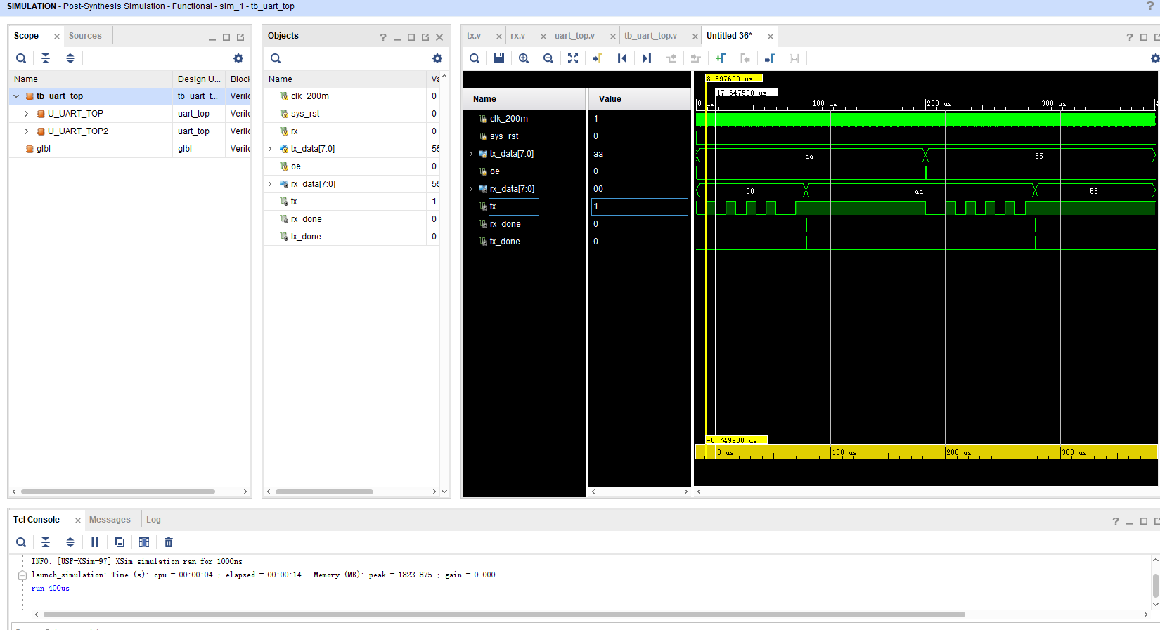
Fig. 6 integrated post simulation