Variation of electron concentration with temperature in semiconductors
Description of experimental principle
Experimental purpose
- Understand the principle of carrier concentration varying with temperature.
- Understand the functions and basic usage of Medici software.
- Master the solution of Fermi level, carrier concentration, electric neutrality condition and incomplete ionization at low temperature.
- The relationship between electron concentration and temperature of n-type semiconductor structure is simulated by Medici software.
- Apply voltage at both ends of the semiconductor, set the temperature, output and record the carrier concentration.
Basic principles
(1) Basic principle of carrier concentration varying with temperature
Fig. 1 shows the schematic diagram of carrier variation with temperature. With the increase of temperature, the carrier concentration is mainly divided into three stages:
- Low temperature weak ionization region. When the temperature is very low, most of the donor impurity energy levels are still occupied by electrons, and only a small amount of donor impurities are ionized. This small amount of electrons enter the conduction band, and the number of electrons transiting from the valence band to the conduction band by intrinsic excitation is less. In other words, in this case, all the electrons in the conduction band are provided by ionized donor impurities. As the temperature increases, the ionization of donor impurities intensifies and the electron concentration in the conduction band increases;
- Strong ionization region. When the temperature rises to a certain extent, all donor or acceptor impurities are ionized. Take N-type semiconductor as an example. At this time, the carrier in the conduction band is basically provided by the electron transition ionized by the donor level to the conduction band, and the electron concentration of intrinsic excitation is very small. Therefore, in this range, the carrier concentration is independent of temperature and always equal to the doping concentration. The temperature range in which the carrier concentration remains equal to the impurity concentration is called the saturation region.
- High temperature intrinsic excitation region. When the temperature continues to rise, the number of intrinsic carriers generated by intrinsic excitation is much more than that generated by impurity ionization, which is the same as that of undoped intrinsic semiconductors. At this time, the Fermi level is close to the center line of the band gap, and the carrier concentration increases rapidly with the increase of temperature. Obviously, the higher the impurity concentration, the higher the temperature at which the intrinsic excitation plays a major role.
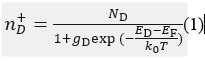
The ionization donor concentration can be obtained by multiplying the state density by the probability of the electron occupying the energy level:
The ionization acceptor concentration is: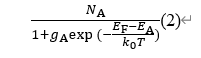
It can be seen from the above two formulas that the relative position between the impurity level and the Fermi level reflects the occupation of the impurity level by electrons and holes, that is, when the Fermi level is far below ED, it can be considered that almost all the donor impurities are ionized. On the contrary, when EF is far above ED, the donor impurity is basically not ionized.
Taking n-type semiconductor as an example, the electrons in its conduction band are negatively charged, the ionized donor impurities are positively charged, and the holes in the valence band are positively charged. Therefore, the electric neutrality condition is:
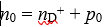
Since intrinsic excitation rarely occurs in the low-temperature weak ionization region, the electric neutrality condition is written as
n0 = nD +, and because ND + is much smaller than ND, it is simplified as follows: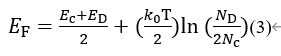
It can be deduced from the formula that when the temperature rises from 0 K, the Fermi level rises rapidly, but the speed is slower and slower. After reaching the extreme value, the Fermi level begins to decline.
When the Fermi level falls below the donor level, most donor impurities are ionized, which is a strong ionization region
Since Nc is greater than ND, the second term is negative. At a certain temperature, the larger the ND, the closer the EF is to the guide band. When ND is constant, the higher the temperature, the closer EF is to the intrinsic Fermi level Ei.
When the temperature is high enough, the thermally excited electrons in the valence band transition to the conduction band, which increases the electron concentration in the conduction band again, and the number of excited electrons continues to increase with the increase of temperature.
Medici simulation code
title concentration

mesh                         //Initialize grid generation
x.mesh width=5 h1=0.1	     //Describe the uniform distribution of the grid 0 ~ 5 in the X direction at an interval of 0.1 μ m from the grid
y.mesh loc=-.1 n=1            //Set the first grid line in the Y direction to -0.1
y.mesh loc=0 n=2             //Set the second grid line in the Y direction at 0 to define the oxide layer thickness
y.mesh depth=1.1 h1=0.1       //Describe the uniform distribution of grid 0 ~ 1.1 in Y direction and 0.1 μ m apart from the grid

regi silicon                    //The material of the defined area is silicon

elec name=A y.max=0          //The name of the description electrode is A, and the position is 0 in the Y direction
elec name=K y.min=1          //The name of the description electrode is K, and the position is 1 in the Y direction

elec name=sink thermal top     //The name of the description electrode is sink thermal placed on the surface
elec name=sink thermal bot     //The name of the description electrode is sink thermal, which is placed at the bottom

prof n.type uniform concen=1.6031e14  //Set the N-type doping concentration to 1.6031e14

regrid doping ratio=2 smooth=1       //The smoothness of the output structure graph is set to 1, and the boundaries of each area remain unchanged
plot.2d grid title="initial grid" fill scale
//The title of the output 2D graph is initial grid, and fill indicates that different areas are filled with colors
plot.2d grid title="grid" fill
//The title of the output 2D graph is grid, and the parameter grid represents the display net list

model incomple temperature=6        //Set the initial simulation temperature to 6K
symb car=2 lat.temp coup.lat           //Input algorithm
meth itlimit=20
impurity name=n-type silicon GB=2 EB0=60e-3
//The impurity type is defined as N type, which is applicable to all SI with degeneracy of 2 and impurity ionization energy of 60e-3eV

solve     //The solution is obtained under the condition of zero bias

extract expr=@n name=n0 condi=(@x=5&&@y=0.5) print
extract expr=@t(sink) name=T condi=(@x=5&&@y=0.5) print

loop steps=400                   //Set the number of steps of a cycle to 400
assign name=k n.value=6 del=2     //The variable name is k, starting from 6 in steps of 2
solve T(sink)=@k
l.end

plot.1d x.ax=T y.ax=n0 sym=15 color=3 left=0 out.f=n02(T)  //One dimensional variation of display parameters
matlab theoretical simulation
syms t;
syms x;
k=1.38e-23;
ec=1.12;
ev=0;
q=1.602e-19;
nc=(5.28e21.*t.^(3/ 2)).*1e-6;
nv=(2.186e21.*t.^(3/2)).*1e-6;
nd=1.6031e16;  %Set doping concentration
ed=1.06;
T=6:2:700;

a=2.*nc.*exp(((-ec-ed).*q)./(k.*t));
b=nc.*exp(((-ec).*q)./(k.*t));
c=2.*nv.*exp(((ev-ed).*q)./(k.*t))+nd;
d=nv.*exp((ev.*q)./(k.*t));
eqn=a.*x^3+b.*x^2-c.*x-d==0;

[d]=solve(eqn,x);
d(2);
ef=(k.*t.*log(d(2)))./q;

y=nc.*exp(((ef-ec).*q)./(k.*t));
z=subs(y,t,T);
r=double(z);

figure
semilogy(T,z)
Variation of mobility with electric field in semiconductors
Description of experimental principle
Experimental purpose
- Understand the basic principle of carrier mobility changing with electric field.
- Understand the functions and basic usage of Medici software.
- Master the change law of mobility under different electric field range.
- Medici is used to simulate the state of n-type semiconductor structure under different electric fields and obtain the change of mobility.
- Voltage is applied at both ends of the semiconductor to output and record the carrier mobility and drift velocity.
Basic principles
Basic principle of the relationship between mobility and electric field in semiconductors:
- When the electric field is not too strong, the relationship between current density and electric field strength obeys Ohm's law. For a given material, the conductivity is constant and independent of the electric field, the average drift velocity is directly proportional to the electric field strength, and the mobility is independent of the electric field. However, when the electric field strength increases to more than 10 ^5 V/cm, the current is no longer proportional to the electric field strength and deviates from Ohm's law. At this time, the conductivity is no longer a constant and changes with the electric field.
- The reason for the deviation of Ohm's law under strong electric field can be explained mainly from the energy exchange process of carrier and lattice vibration scattering. In the absence of external electric field, when the carrier and lattice scatter, they will absorb phonons or emit phonons, exchange momentum and energy with the lattice, the net energy exchanged is zero, the average energy of the carrier is the same as that of the lattice, and they are in thermal equilibrium.
- When the electric field exists, the carrier obtains energy from the electric field, and then transmits the energy to the lattice in the form of emitting phonons. At this time, on average, the number of phonons emitted by the carrier is more than the number of phonons absorbed. When reaching the steady state, the energy obtained by the carrier per unit time from the electric field is the same as that given to the lattice. However, in the case of strong electric field, the carrier obtains a lot of energy from the electric field, and the average energy of the carrier is greater than that in the thermal equilibrium state, so the carrier and lattice system are no longer in the thermal equilibrium state. Temperature is a measure of the average kinetic energy. Since the energy of the carrier is greater than that of the lattice system, the effective temperature Te of the carrier is introduced to describe the carriers in the lattice system that are not in thermal equilibrium, and the carriers in this state are called hot carriers. Therefore, in the case of strong electric field, the carrier temperature Te is higher than the lattice temperature T, and the average energy of the carrier is greater than that of the lattice. When the hot carrier scatters with the lattice, due to the high energy of the hot carrier, the velocity is greater than that in the thermal equilibrium state. It can be seen from the fact that the average free time is equal to the average free path divided by the carrier velocity that the average free time decreases and the mobility decreases when the average free path remains unchanged.
- When the electric field is not very strong, the carrier mainly scatters with the acoustic wave, and the mobility decreases. When the electric field is further enhanced and the carrier energy is high enough to be compared with the optical wave phonon energy, the optical wave phonon can be emitted during scattering, so most of the energy obtained by the carrier disappears, so the average drift velocity can reach saturation.
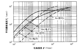
- Fig. 2 shows the relationship between the average drift velocity of germanium and silicon and the electric field intensity. It can be seen from the figure that when the electric field is not strong, the average drift velocity has a linear relationship with the electric field strength, then the slope decreases, and finally the drift velocity reaches saturation
Medici simulation code
title mobility/velocity
mesh                        //Initialize grid generation
x.mesh width=5 h1=0.1        //Describe the uniform distribution of the grid 0 ~ 5 in the X direction at an interval of 0.1 μ m from the grid
y.mesh loc=-.1 n=1           //Set the first grid line in the Y direction to -0.1
y.mesh loc=0 n=2            //Set the second grid line in the Y direction at 0 to define the oxide layer thickness
y.mesh depth=1.1 h1=0.1     //Describe the uniform distribution of grid 0 ~ 1.1 in Y direction and 0.1 μ m apart from the grid

regi silicon                  //The material of the defined area is silicon

elec name=A y.max=0        //The name of the description electrode is A, and the position is 0 in the Y direction
elec name=K y.min=1        //The name of the description electrode is K, and the position is 1 in the Y direction

prof n.type uniform concen=1.6031e14 //Set the N-type doping concentration to 1.6031e14

regrid doping ratio=2 smooth=1       //Output structure graphics
plot.2d grid title="initial grid" fill scale   //The output 2D drawing is titled initial grid
plot.2d grid title="grid" fill             //The output 2D drawing is titled grid

model analytic fldmob                //Input algorithm
symb car=2
meth itlimit=20
solve                               //The solution is obtained under the condition of zero bias

extract expression=@n.mobil       name=mun condition=(@x=5&&@y=0.5) print
extract expression=@em           name=Em condition=(@x=5&&@y=0.5) print
extract expression=@em*@n.mobil  name=vd condition=(@x=5&&@y=0.5) print

solve
solve elec=A vstep=0.01 nstep=100
solve elec=A vstep=0.1 nstep=90
solve elec=A vstep=1 nstep=90
solve elec=A vstep=2 nstep=50
solve elec=A vstep=6 nstep=50
plot.1d x.ax=Em y.ax=mun sym=2 out.f=mun(E) x.log        //Output one-dimensional graphic results
plot.1d x.ax=Em y.ax=vd  sym=2 out.f=vd(E) x.log y.log

plot.1d x.ax=Em y.ax=mun sym=2 color=2 left=-1e6 bot=-0.25e3 out.f=mun2(E)
plot.1d x.ax=Em y.ax=vd  sym=2 color=3 left=-1e5 right=2e5 out.f=vd2(E)
matlab theoretical simulation
mum_min=55.25;
mum_max=1429.23;
nrefn=1.072e17;
nrefn_2=1e30;
num=-2.3;
xin=-3.8;
a=0.73;
b=2;
N=1.6031e16;
T=25+273.15;
E=0:1000:1e6;

u_n=(mum_min +  mum_max*(T/300)^num - mum_min)/1+(T/300)^xin*((N/nrefn)^a +(N/nrefn_2)^3);
v_sat=2.4*10^7/1+0.8*exp(T/600);
u=u_n./(1+(u_n.*E./v_sat).^b).^(1./b);

figure(1)
subplot(2,1,1);
plot(E,u,'-ro','MarkerSize',2);

grid on % grid
title('mobility\mu');
xlabel('E(V/cm)');
ylabel('\mu(cm^2/Vs)');

vel=u.*E;
subplot(2,1,2);
plot(E,vel,'-b*','MarkerSize',2);

grid on
title('Drift velocity');
xlabel('E(V/cm)');
ylabel('vd(cm/s)');
Effect display: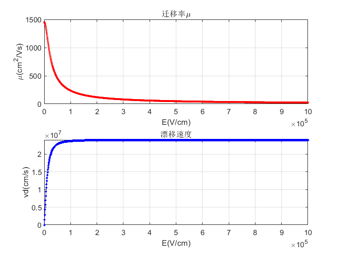
appendix
This article is used to record semiconductor physics software experiments. The experimental code comes from the same group of students. The experimental code about MIS structure is still being sorted out and will be supplemented as soon as possible.