tinyriscv, the core cpu part of SoC project, is designed with the classic three-stage pipeline structure, which is well-known: value - > decoding - > execution three-stage pipeline.
The decoding module was annotated in the last blog post. Now let's introduce the execution module:
catalogue
1. Annotation of execution module
2. ex.v (combinational logic circuit)
2.2 multiplication operation annotation
3. ram. Temporary data storage: v.
1. Annotation of execution module
The executive part of RISC-V kernel: involving ex.v and ram v. div.v and other modules. div.v will be described in detail in the next chapter.
Detailed structure diagram of executive part:
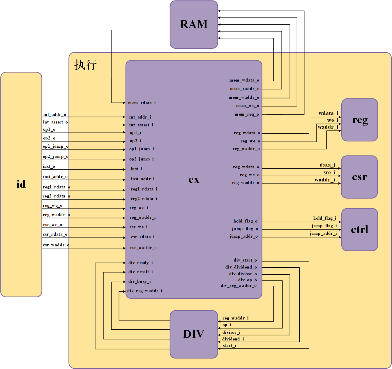
Next, the execution structure is annotated in modules:
2. ex.v (combinational logic circuit)
The main functions are:
1. Execute the corresponding operation according to the current instruction (addition, subtraction, multiplication, division, shift, etc.), such as the add instruction, add the value of register 1 and the value of register 2. Note: the execution of other instructions is similar. It should be noted that the signals not involved should be set to the default value, and the if and case conditions should be written completely to avoid latch.
2. If it is a jump instruction, send a jump signal.
3. If it is a memory loading instruction, read the memory data of the corresponding address.
Interface signals and notes:
// from id
    input wire[`InstBus] inst_i,            // Instruction content
    input wire[`InstAddrBus] inst_addr_i,   // Instruction address
    input wire reg_we_i,                    // Write general purpose register
    input wire[`RegAddrBus] reg_waddr_i,    // Write general register address
    input wire[`RegBus] reg1_rdata_i,       // General register 1 input data
    input wire[`RegBus] reg2_rdata_i,       // General register 2 input data
    input wire csr_we_i,                    // Whether to write CSR register
    input wire[`MemAddrBus] csr_waddr_i,    // Write CSR register address
    input wire[`RegBus] csr_rdata_i,        // CSR register input data
    input wire int_assert_i,                // Interrupt occurrence flag
    input wire[`InstAddrBus] int_addr_i,    // Interrupt jump address
    input wire[`MemAddrBus] op1_i,
    input wire[`MemAddrBus] op2_i,
    input wire[`MemAddrBus] op1_jump_i,
    input wire[`MemAddrBus] op2_jump_i,

    // from mem
    input wire[`MemBus] mem_rdata_i,        // Memory input data

    // from div
    input wire div_ready_i,                 // Division completion flag
    input wire[`RegBus] div_result_i,       // Division result
    input wire div_busy_i,                  // Division busy flag
    input wire[`RegAddrBus] div_reg_waddr_i,// Register address to be written after division

    // to mem
    output reg[`MemBus] mem_wdata_o,        // Write memory data
    output reg[`MemAddrBus] mem_raddr_o,    // Read memory address
    output reg[`MemAddrBus] mem_waddr_o,    // Write memory address
    output wire mem_we_o,                   // Do you want to write memory
    output wire mem_req_o,                  // Request access memory flag

    // to regs
    output wire[`RegBus] reg_wdata_o,       // Write register data
    output wire reg_we_o,                   // Do you want to write the general register
    output wire[`RegAddrBus] reg_waddr_o,   // Write general register address

    // to csr reg
    output reg[`RegBus] csr_wdata_o,        // Write CSR register data
    output wire csr_we_o,                   // Do you want to write CSR register
    output wire[`MemAddrBus] csr_waddr_o,   // Write CSR register address

    // to div
    output wire div_start_o,                // Start division flag
    output reg[`RegBus] div_dividend_o,     // Divisor
    output reg[`RegBus] div_divisor_o,      // Divisor
    output reg[2:0] div_op_o,               // Which division instruction is it
    output reg[`RegAddrBus] div_reg_waddr_o,// Register address to be written after division

    // to ctrl
    output wire hold_flag_o,                // Pause flag
    output wire jump_flag_o,                // Jump flag
    output wire[`InstAddrBus] jump_addr_o   // Jump to destination address
2.1 execute code parsing
(refer to the original author's blog):
Next, take the add instruction as an example. The function of the add instruction is to add the value of register 1 and the value of register 2, and finally write the result to the destination register. The code is as follows:
...

`INST_TYPE_R_M: begin
     if ((funct7 == 7'b0000000) || (funct7 == 7'b0100000)) begin
         case (funct3)
             `INST_ADD_SUB: begin
                 jump_flag = `JumpDisable;
                 hold_flag = `HoldDisable;
                 jump_addr = `ZeroWord;
                 mem_wdata_o = `ZeroWord;
                 mem_raddr_o = `ZeroWord;
                 mem_waddr_o = `ZeroWord;
                 mem_we = `WriteDisable;
                 if (inst_i[30] == 1'b0) begin
                     reg_wdata = reg1_rdata_i + reg2_rdata_i;
                 end else begin
                     reg_wdata = reg1_rdata_i - reg2_rdata_i;
                 end
        ...
     end
...
Lines 2 to 4, decoding operation.
Line 5, process the add or sub instruction.
In lines 6 to 12, operations not involved in the current instruction (such as jump, write memory, etc.) need to be set back to the default value.
In line 13, the 30th bit in the instruction code distinguishes whether it is an add instruction or a sub instruction. 0 indicates the add instruction and 1 indicates the sub instruction.
Line 14, perform the addition operation.
Line 16, perform subtraction.
The execution of other instructions is similar. It should be noted that the signals not involved should be set to the default value, and the if and case conditions should be written completely to avoid latch.
The execution of the jump instruction is described below with the beq instruction. The coding of beq instruction is as follows:
The function of beq instruction is to jump when the value of register 1 is equal to that of register 2. The destination address of jump is the address of current instruction plus the value of symbol extended imm. The specific codes are as follows:
...
`INST_TYPE_B: begin
case (funct3)
`INST_BEQ: begin
hold_flag = `HoldDisable;
mem_wdata_o = `ZeroWord;
mem_raddr_o = `ZeroWord;
mem_waddr_o = `ZeroWord;
mem_we = `WriteDisable;
reg_wdata = `ZeroWord;
if (reg1_rdata_i == reg2_rdata_i) begin
jump_flag = `JumpEnable;
jump_addr = inst_addr_i + {{20{inst_i[31]}}, inst_i[7], inst_i[30:25], inst_i[11:8], 1'b0};
end else begin
jump_flag = `JumpDisable;
jump_addr = `ZeroWord;
end
...
end
...
Lines 2 to 4 decode the beq instruction.
Lines 5 to 10, set the signal not involved as the default value.
In line 11, judge whether the value of register 1 is equal to the value of register 2.
Line 12, jump enable, that is, jump occurs.
Line 13, calculate the destination address of the jump.
Lines 15 and 16, no jump occurs.
The execution of other jump instructions is similar and will not be repeated here.
Please refer to the original author's blog for the analysis of relevant codes and concepts related to memory access and writeback operations.
Write RISC-V processor from scratch
Write the blog of RISC-V processor | liangkangnan from scratch (gitee.io) https://liangkangnan.gitee.io/2020/04/29/%E4%BB%8E%E9%9B%B6%E5%BC%80%E5%A7%8B%E5%86%99RISC-V%E5%A4%84%E7%90%86%E5%99%A8/ It should be noted that in the write back operation, when writing data to the memory, you need to read the data in the memory first, modify it, and then write it in. (for example, the sb instruction only changes the corresponding bytes in the read 32-bit memory data, and the data of the other 3 bytes remains unchanged, and then is written back to memory.)
The Load and Store instructions of RV32I not only provide the loading and storage of 32-bit words (lw, sw), but also support the loading of signed and unsigned bytes and halfwords (lb, lbu, lh, lhu) and the storage of bytes and halfwords (sb, sh). Signed bytes and halfword symbols are extended to 32 bits and then written to the destination register. Even if the natural data type is narrower, the low bit width data is expanded and then processed, which enables the subsequent integer calculation instructions to correctly process all 32 bits. Unsigned bytes and halfwords commonly used in text and unsigned integers are unsigned extended to 32 bits before writing to the target register.
Half word loading instruction has lh symbol:
`INST_LH: begin
    jump_flag = `JumpDisable;
    hold_flag = `HoldDisable;
    jump_addr = `ZeroWord;
    mem_wdata_o = `ZeroWord;
    mem_waddr_o = `ZeroWord;
    mem_we = `WriteDisable;
    mem_req = `RIB_REQ;
    mem_raddr_o = op1_add_op2_res;
    if (mem_raddr_index == 2'b0) begin
        reg_wdata = {{16{mem_rdata_i[15]}}, mem_rdata_i[15:0]};
    end else begin
        reg_wdata = {{16{mem_rdata_i[31]}}, mem_rdata_i[31:16]};
    end
end
In ` Inst_ In the LH instruction, the data read out from the memory in lines 11 and 13 is expanded in sign bits for the following reasons: for immediate numbers less than 32 bits, if the immediate number (negative number) is directly stored in the 32-bit register (low order), the highest order will be automatically supplemented with 0, The value of the immediate data will be changed (because the program directly judges the highest bit each time when judging the positive and negative).
Load unsigned halfword instruction lhu:
`INST_LHU: begin
    jump_flag = `JumpDisable;
    hold_flag = `HoldDisable;
    jump_addr = `ZeroWord;
    mem_wdata_o = `ZeroWord;
    mem_waddr_o = `ZeroWord;
    mem_we = `WriteDisable;
    mem_req = `RIB_REQ;
    mem_raddr_o = op1_add_op2_res;
    if (mem_raddr_index == 2'b0) begin
        reg_wdata = {16'h0, mem_rdata_i[15:0]};
    end else begin
        reg_wdata = {16'h0, mem_rdata_i[31:16]};
    end
end
In ` Inst_ In the LHU instruction, the data read out from the memory in lines 11 and 13 are expanded by unsigned bits. Because the operation is an unsigned number and there is no sign bit, the high bit is directly filled with zero.
2.2 multiplication operation annotation
Next, the multiplication operation of the execution module is annotated. The main code of the multiplication operation is as follows:
//Processing multiplication instructions (all data in the hardware is stored in the form of complement!!!)
always @ (*) begin
    //According to opcode and funct7, it is determined that the instruction is a multiplication operation
    if ((opcode == `INST_TYPE_R_M) && (funct7 == 7'b0000001)) begin
        case (funct3)//Determine the specific multiplication instruction according to funct3
            `INST_MUL, `INST_MULHU: begin
                mul_op1 = reg1_rdata_i;
                mul_op2 = reg2_rdata_i;
            end
            //The mulhsu instruction multiplies the 32-bit integer in the operand register rsl and rs2
            //Where rsl is regarded as signed number and rs2 is regarded as unsigned number, and the high 32 bits of the result are written back to register rd
            `INST_MULHSU: begin
                //The signed number is multiplied by the unsigned number, and the signed number is inversely added by 1
                mul_op1 = (reg1_rdata_i[31] == 1'b1)? (reg1_data_invert): reg1_rdata_i;
                mul_op2 = reg2_rdata_i;
            end
            //The mulh instruction multiplies 32-bit integers in the operand registers rsl and rs2 as signed numbers
            //The upper 32 bits of the result are written back to register rd.
            `INST_MULH: begin
                //Signed number multiplication, which takes both operands and adds 1 inversely
                mul_op1 = (reg1_rdata_i[31] == 1'b1)? (reg1_data_invert): reg1_rdata_i;
                mul_op2 = (reg2_rdata_i[31] == 1'b1)? (reg2_data_invert): reg2_rdata_i;
            end
            default: begin
                mul_op1 = reg1_rdata_i;
                mul_op2 = reg2_rdata_i;
            end
        endcase
    end else begin
        mul_op1 = reg1_rdata_i;
        mul_op2 = reg2_rdata_i;
    end
end
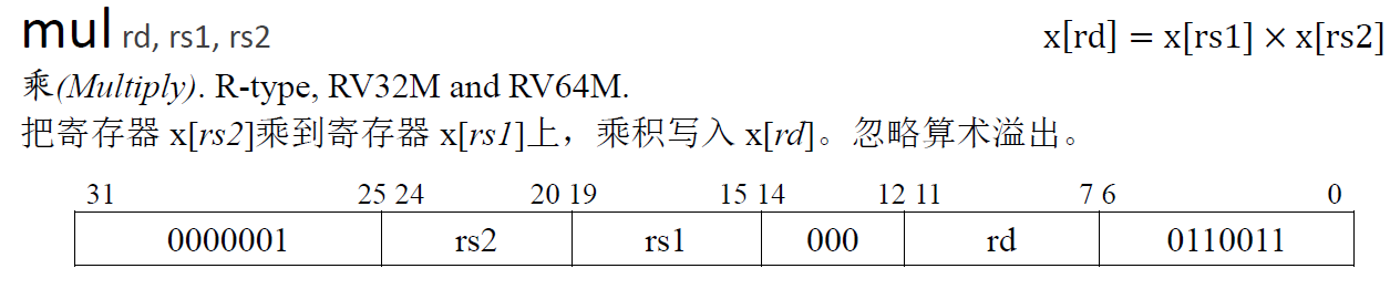
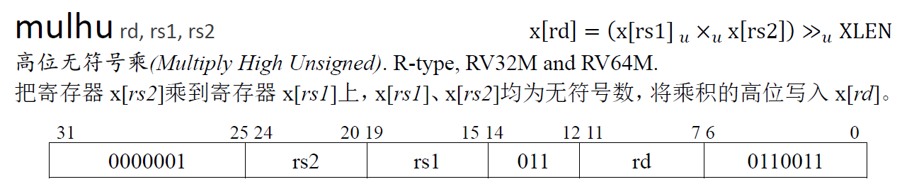
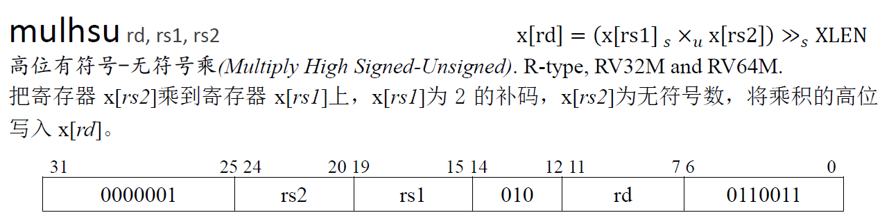
First, briefly introduce the four multiplication instructions involved in the code.
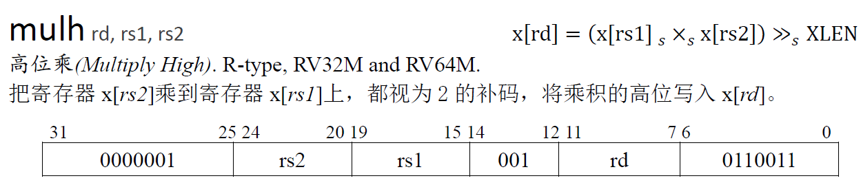
`INST_MUL: unsigned number * unsigned number. Write the low order of the product into x[rd]. The specific instruction format is as follows
`INST_MULHU: unsigned number * unsigned number. Write the high bit of the product into x[rd]. The specific instruction format is as follows
`INST_MULHSU: signed number * unsigned number. Write the high bit of the product into x[rd]. The specific instruction format is as follows
`INST_MULH: signed number * signed number. Write the high bit of the product into x[rd]. The specific instruction format is as follows
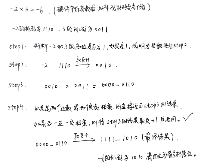
Disassemble and analyze the multiplication operation step by step (take the instruction mulh as an example, and other instructions are similar):
Step1:
`INST_MULH: begin
    //Signed number multiplication, which takes both operands and adds 1 inversely
    mul_op1 = (reg1_rdata_i[31] == 1'b1)? (reg1_data_invert): reg1_rdata_i;
    mul_op2 = (reg2_rdata_i[31] == 1'b1)? (reg2_data_invert): reg2_rdata_i;
end
Step 2: first judge whether the multiplier and multiplicand are negative numbers. If they are negative numbers, you need to convert the negative numbers:
assign reg1_data_invert = ~reg1_rdata_i + 1;
assign reg2_data_invert = ~reg2_rdata_i + 1;
Step3: multiply the above converted results
assign mul_temp = mul_op1 * mul_op2;
Step4: if two positive numbers or two negative numbers are multiplied, the result of Step3 will be returned directly; If it is a positive negative multiplication, the result of Step3 is taken inversely plus one.
assign mul_temp_invert = ~mul_temp + 1; //Reverse the complement of a negative number and add 1.
With - 2 × 3 = - 6 as an example, the multiplication process is as follows:
Store the high bit of the result in the register:
//The mulh instruction multiplies 32-bit integers in the operand registers rsl and rs2 as signed numbers
//The upper 32 bits of the result are written back to register rd.
`INST_MULH: begin
    jump_flag = `JumpDisable;
    hold_flag = `HoldDisable;
    jump_addr = `ZeroWord;
    mem_wdata_o = `ZeroWord;
    mem_raddr_o = `ZeroWord;
    mem_waddr_o = `ZeroWord;
    mem_we = `WriteDisable;
    case ({reg1_rdata_i[31], reg2_rdata_i[31]})
        2'b00: begin
            reg_wdata = mul_temp[63:32];
        end
        2'b11: begin
            reg_wdata = mul_temp[63:32];
        end
        2'b10: begin
            reg_wdata = mul_temp_invert[63:32];
        end
        default: begin
            reg_wdata = mul_temp_invert[63:32];
        end
    endcase
end
3. ram.v
Function: store temporary data.
For code analysis, see the introduction of rom in the chapter of taking instructions. The two codes are the same
1, RISC-V kernel structure - take the following:https://blog.csdn.net/weixin_42294124/article/details/123033894?spm=1001.2014.3001.5502
`include "../core/defines.v" // ram module module ram( input wire clk, input wire rst, input wire we_i, // write enable input wire[`MemAddrBus] addr_i, // addr input wire[`MemBus] data_i, output reg[`MemBus] data_o // read data ); reg[`MemBus] _ram[0:`MemNum - 1]; //Write RAM always @ (posedge clk) begin if (we_i == `WriteEnable) begin //The address entered from the kernel changes at intervals of 0, 4, 8 and C, //In order to store data in RAM in sequence (0,1,2,3...) In the address, //Therefore, the upper 30 bits of the address are used as the input address. _ram[addr_i[31:2]] <= data_i; end end //Read RAM always @ (*) begin if (rst == `RstEnable) begin data_o = `ZeroWord; end else begin data_o = _ram[addr_i[31:2]];//Address addr in RAM_ Data readout in I [31:2] end end endmodule
reference resources:
Write the blog of RISC-V processor | liangkangnan from scratch (gitee.io)