1, Experimental principle
1. Single cycle CPU
Single cycle CPU can be regarded as composed of data path and control unit. Data path refers to the path through which data passes and the functional components involved in the path during the execution of instructions. The control unit generates different control signals for different data paths according to the different functions of each instruction to correctly control the execution process of the instruction.
Therefore, to design a processor, we first need to determine the instruction set and instruction code of the processor, then determine the data path of each instruction, and finally determine the control signal of the data path.
2. Single cycle CPU instruction module
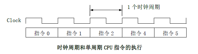
Single Cycle CPU means that the CPU only needs one clock cycle from taking out an instruction to executing the instruction. The execution process of an instruction includes: fetch instruction → analyze instruction → execute instruction → save result (if any). For a Single Cycle CPU, these execution steps are completed in one clock cycle.
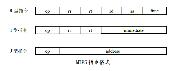
3. MIPS instruction format
MIPS instruction system structure includes MIPS-32 and MIPS-64. MIPS-32 is selected as MIPS instruction in this experiment. The MIPs instructions mentioned below refer to MIPS-32. The instruction format of MIPs is 32 bits. The following figure shows three formats of MIPs instructions.
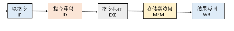
4. Instruction processing flow
5. Single cycle CPU data path
The circuit of CPU includes two parts: Data path and Control Unit. The overall design diagram of single cycle CPU is given below.
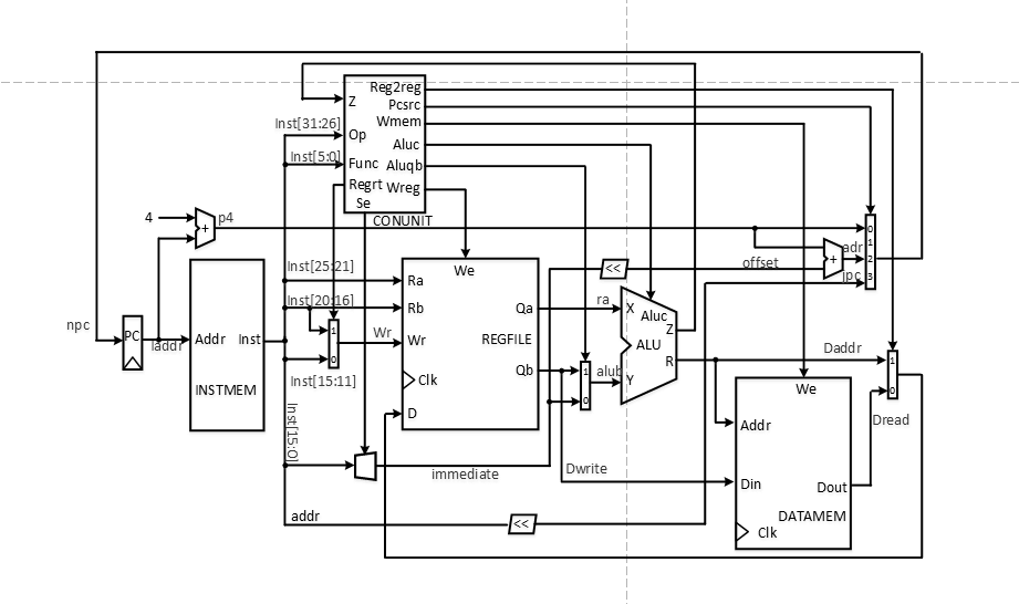
A simple data path and necessary control circuit diagram that can basically complete the required command function in a single cycle. The instruction is stored in the instruction memory and the data is stored in the data memory. When accessing the memory, the address is given first, and then controlled by the read / write signal. For the register group, when reading, the address is given first, and the output end directly outputs the corresponding data; During the write operation, when the We enable signal is 1, the write is triggered at the edge of the clock.
2, Design of single cycle CPU
1.pcadd4
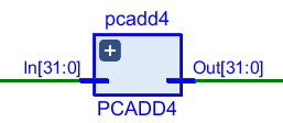
pcadd4 is used as the update signal of PC register.
Since each instruction is 32 bits, a 32-bit adder is added to add it to the 32-bit immediate number 4, and the result is updated into the PC register at the rising edge of the current clock signal.
Where, In is the input port, and enter the current instruction address; Out is the address of the next instruction and the output port.
① PCADD4
module PCadd4(PC_o,PCadd4);
    input [31:0] PC_o;//Offset
    output [31:0] PCadd4;//New instruction address
    CLA_32 cla32(PC_o,4,0, PCadd4, Cout);
endmodule
② CLA_32
module CLA_32(X,Y,Cin,S,Cout);
    input[31:0]X,Y;
    input Cin;
    output[31:0]S;
    output Cout;
    wire Cout0,Cout1,Cout2,Cout3,Cout4,Cout5,Cout6;
    CLA_4 add0(X[3:0],Y[3:0],Cin,S[3:0],Cout0);
    CLA_4 add1(X[7:4],Y[7:4],Cout0,S[7:4],Cout1);
    CLA_4 add2(X[11:8],Y[11:8],Cout1,S[11:8],Cout2);
    CLA_4 add3(X[15:12],Y[15:12],Cout2,S[15:12],Cout3);
    CLA_4 add4(X[19:16],Y[19:16],Cout3,S[19:16],Cout4);
    CLA_4 add5(X[23:20],Y[23:20],Cout4,S[23:20],Cout5);
    CLA_4 add6(X[27:24],Y[27:24],Cout5,S[27:24],Cout6);
    CLA_4 add7(X[31:28],Y[31:28],Cout6,S[31:28],Cout);
endmodule
③ CLA_4
module CLA_4(X,Y,Cin,S,Cout);
    input [3:0]X,Y;
    output Cout;
    input Cin;
    output [3:0]S;
    and i0(Y_3,X[3],Y[3]);
    or i1(X_3,X[3],Y[3]);
    and i2(Y_2,X[2],Y[2]);
    or i3(X_2,X[2],Y[2]);
    and i4(Y_1,X[1],Y[1]);
    or i5(X_1,X[1],Y[1]);
    and i6(Y_0,X[0],Y[0]);
    or i7(X_0,X[0],Y[0]);
    not i01(Y_31,Y_3);
    nand i02(Y_32,X_3,Y_2);
    nand i03(Y_33,X_3,X_2,Y_1);
    nand i04(Y_34,X_3,X_2,X_1,Y_0);
    nand i05(Y_35,X_3,X_2,X_1,X_0,Cin);
    nand i00(Cout,Y_31,Y_32,Y_33,Y_34,Y_35);//Implementation of Cout's output gate circuit
    not i_2(Y__3,Y_3);
    and i21(Y_21,Y__3,X_3);
    not i22(Y_22,Y_2);
    nand i23(Y_23,X_2,Y_1);
    nand i24(Y_24,X_2,X_1,Y_0);
    nand i25(Y_25,X_2,X_1,X_0,Cin);
    nand i26(Y_26,Y_22,Y_23,Y_24,Y_25);
    xor i20(S[3],Y_21,Y_26);//Implementation of output gate circuit of S3
    not i_1(Y__2,Y_2);
    and i11(Y_11,Y__2,X_2);
    not i12(Y_12,Y_1);
    nand i13(Y_13,X_1,Y_0);
    nand i14(Y_14,X_1,X_0,Cin);
    nand i15(Y_15,Y_12,Y_13,Y_14);
    xor i10(S[2],Y_11,Y_15);//Realization of output gate circuit of S2
    not i_0(Y__1,Y_1);
    and i51(Y_51,Y__1,X_1);
    not i52(Y_52,Y_0);
    nand i53(Y_53,X_0,Cin);
    nand i54(Y_54,Y_52,Y_53);
    xor i50(S[1],Y_51,Y_54);//Output gate circuit of S1
    not i41(Y__0,Y_0);
    and i42(Y_4,Y__0,X_0);
    xor i40(S[0],Y_4,Cin);//Output gate circuit of S0
endmodule
2. PC
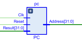
The PC register is used to give the address of the instruction in the instruction memory.
In order to achieve stable output, the rising edge of the clock signal is updated, and a control signal is required. When the control signal is 0, initialize the PC register, that is, set all to zero.
Where, Clk is the input signal and the clock cycle; Reset is the input signal and the input control signal; Result is the input signal and the input target address, which may be the jump address or the address of the next instruction; Address is the output signal and the output instruction address.
The codes are as follows:
module PC(Clk,Reset,Result,Address);
    input Clk;//Clock
    input Reset;//Whether to reset the address. 0 - initialize PC, otherwise accept new address
    input[31:0] Result;
    output reg[31:0] Address;
    initial begin
        Address  <= 0;
    end
    always @(posedge Clk or negedge Reset)
    begin
        if (Reset==0) //If 0, initialize the PC, otherwise accept the new address
            begin
                Address <= 0;
            end
        else
            begin
                Address =  Result;
        end
    end
endmodule
3.INSTMEM
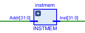
According to the current pc, read the instruction with the corresponding address Addr[6:2] in the instruction register.
Take the input of pc as a sensitive variable. When the pc changes, read the instruction, and output the corresponding instruction in the instruction register according to the relevant address. When designing the instruction, 12 given instructions should be used and as reasonable as possible.
Addr is the input signal and the input instruction address; Inst is the output signal and the output instruction code.
The codes are as follows:
module INSTMEM(Addr,Inst);//Instruction memory
    input[31:0]Addr;
    //If the status is' 0 ', write the instruction register; otherwise, read the instruction register
    output[31:0]Inst;
    wire[31:0]Rom[31:0];
    assign Rom[5'h00]=32'h20010008;//addi $1,$0,8 $1=8
    assign Rom[5'h01]=32'h3402000C;//ori $2,$0,12 $2=12
    assign Rom[5'h02]=32'h00221820;//add $3,$1,$2 $3=20
    assign Rom[5'h03]=32'h00412022;//sub $4,$2,$1 $4=4
    assign Rom[5'h04]=32'h00222824;//and $5,$1,$2 $5=8
    assign Rom[5'h05]=32'h00223025;//or $6,$1,$2 $6=12
    assign Rom[5'h06]=32'h14220002;//bne $1,$2,2
    assign Rom[5'h07]=32'hXXXXXXXX;
    assign Rom[5'h08]=32'hXXXXXXXX;
    assign Rom[5'h09]=32'h10220002;// beq $1,$2,2
    assign Rom[5'h0A]=32'h0800000D;// J 0D
    assign Rom[5'h0B]=32'hXXXXXXXX;
    assign Rom[5'h0C]=32'hXXXXXXXX;
    assign Rom[5'h0D]=32'hAD02000A;// sw $2 10($8) memory[$8+10]=10
    assign Rom[5'h0E]=32'h8D04000A;//lw $4 10($8) $4=12
    assign Rom[5'h0F]=32'h00221826;//xor $3,$1,$2
    assign Rom[5'h10]=32'h00021900;//sll $3,$2,4
    assign Rom[5'h11]=32'h00021902;//srl $3,$2,4
    assign Rom[5'h12]=32'h00021903;//sra $3,$2,4
    assign Rom[5'h13]=32'h30470009;//andi $7,$2,9
    assign Rom[5'h14]=32'h382300EF;//xori $3,$1,0xef
    assign Rom[5'h15]=32'h3C011234;//lui $1,0x1234
    assign Rom[5'h16]=32'h0C00001A;//Jal 1A
    assign Rom[5'h17]=32'h0800001A;// J 1A
    assign Rom[5'h18]=32'hXXXXXXXX;
    assign Rom[5'h19]=32'hXXXXXXXX;
    assign Rom[5'h1A]=32'h03E00008;//Jr 16
    assign Rom[5'h1B]=32'hXXXXXXXX;
    assign Rom[5'h1C]=32'hXXXXXXXX;
    assign Rom[5'h1D]=32'hXXXXXXXX;
    assign Rom[5'h1E]=32'hXXXXXXXX;
    assign Rom[5'h1F]=32'hXXXXXXXX;
    assign Inst=Rom[Addr[6:2]];
endmodule
4. DATAMEM
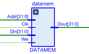
The data memory reads or writes the data register through the control signal, and the module additionally combines the data selector of the output dB, and the module outputs the data DB written back to the register group at the same time.
Since it is necessary to support fetch / save instructions, the data write port for writing data and write enable signal should be added on the basis of instruction memory. Because the write operation is on the rising edge of the clock signal, the clock signal should be added.
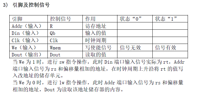
The codes are as follows:
module DATAMEM(Addr,Din,Clk,We,Dout);
    input [31:0]Addr,Din;
    input Clk,We;
    output [31:0]Dout;
	reg [31:0]ram[0:31];
	integer i;
	initial begin
        for ( i = 0 ; i <= 31 ; i = i + 1)
            ram [i] = i;
    end
	always @ (posedge Clk) begin
        if (We) ram[Addr[6:2]] <= Din;
	end
	assign Dout = ram[Addr[6:2]];
endmodule
5. DATAMEM
3, Design and operation results
summary
Tip: here is a summary of the article:
For example, the above is what we want to talk about today. This paper only briefly introduces the use of pandas, which provides a large number of functions and methods that enable us to process data quickly and conveniently.