Catalogue of series articles
(1) Designing RISC-V processor from scratch -- instruction system
(2) Design RISC-V processor from scratch -- Design of single cycle processor
(3) Designing RISC-V processor from scratch -- Simulation of single cycle processor
(4) Designing RISC-V processor from scratch -- Optimization of ALU
preface
In the previous three articles, we have completed the design of single cycle CPU. From this article, we will optimize the single cycle CPU.
The first is to optimize Alu components, because Alu is one of the most important components of CPU, and all operations are carried out here. Previously, we divided the ALU operation unit into arithmetic operation unit (adder), shift operation (shifter), less than one (comparator) and logic operation (logic gate). In the previous design, the adder is directly implemented with the operator "+" in verilog, and the shifter is directly implemented with the operators "> >, < <" in verilog. This is equivalent to giving the design of adder and shifter to the comprehensive tool to complete automatically. The performance of Alu designed in this way is beyond our control. Therefore, this article introduces the optimization of adder and shifter.
1, Design of adder
There are many kinds of common adders. Interested readers can learn by themselves. Here we mainly introduce two kinds of adders: traveling wave carry adder and lead carry adder.
The traveling wave carry adder is composed of n one bit full adders in series. The structure is very simple. The carry output of the upper stage is connected to the carry input of the next stage. This adder has a simple structure and uses few logic resources. However, due to serial calculation, the result of the next level depends on the carry output of the previous level. Therefore, for multi bit adders, it takes a long time to calculate one addition.
If the carry output of each stage can be calculated in advance, the delay can be effectively shortened, which is the so-called carry ahead adder.
Let's start the analysis.
First, list the truth table of one bit full adder
| Ai | Bi | Ci | Si | Ci+1 |
|---|---|---|---|---|
| 0 | 0 | 0 | 0 | 0 |
| 0 | 0 | 1 | 1 | 0 |
| 0 | 1 | 0 | 1 | 0 |
| 0 | 1 | 1 | 0 | 1 |
| 1 | 0 | 0 | 1 | 0 |
| 1 | 0 | 1 | 0 | 1 |
| 1 | 1 | 0 | 0 | 1 |
| 1 | 1 | 1 | 1 | 1 |
The following relationship can be obtained from the truth table:
Si=Ai ^ Bi ^ Ci;
Ci+1=Bi&Ci + Ai&Ci + Ai&Bi=Ai&Bi + (Ai + Bi)&Ci=Gi + Pi&Ci;
Here, two new signals are defined: GI = AI & Bi, pi = AI | Bi;
Gi is called carry generation signal and Pi is called carry transmission signal.
When Gi is 1, carry must be generated, that is, Ci+1 must be 1;
When Gi is 0 and Pi is 1, carry is passed, that is, the value of Ci is passed to Ci+1. When CI is 0, Ci+1 is 0, and Ci+1 is 1.
The carry signal of each stage is represented as follows:
C0=Cin;
C1=A0&B0+(A0+B0)&C0=G0+P0&C0
C2=G1+P1&C1=G1+P1&(G0+P0&C0)=G1+P1&G0+P0&P1&C0
C3=G2+P2&C2=G2+P2&G1+P2&P1&G0+P2&P1&P0&C0
C4=G3+P3&G2+P3&P2&G1+P3&P2&P1&G0+P3&P2&P1&P0&C0
......
As can be seen from the above formula, in this way, the carry signal of each stage only depends on Pi,Gi and C0, so we can calculate the carry signal Ci of each stage and Si of each stage according to the addend A, the addend B and the carry signal C0.
Through the above analysis, it can be concluded that:
Traveling wave adder, serial calculation, simple structure (small area) and large delay
Carry ahead adder, parallel computing, complex structure (large area) and small delay.
If you want to design a high-performance 32-bit adder, you can theoretically generate all Si and Ci in parallel at the same time, but this will make the circuit structure very complex and greatly increase the fan in and fan out of the circuit, which is not feasible in the actual design.
Therefore, we implement a 32-bit adder in the way of intra group parallel and inter group parallel, that is, first implement a 4-bit carry ahead adder, then implement a 16 bit carry ahead adder in parallel between four 4-bit carry ahead adders, and then implement a 32-bit carry ahead adder in parallel between two 16 bit carry ahead adders.
Its structure is as follows:
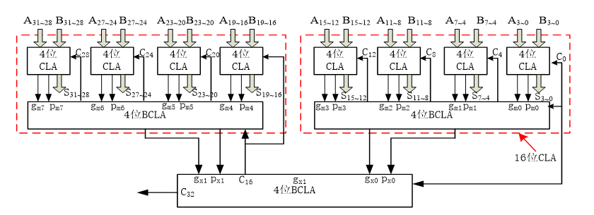
The implementation code is as follows:
//4-bit CLA component
module cla_4(p,g,c_in,c,gx,px);
input[3:0] p,g;
input c_in;
output[4:1] c;
output gx,px;

assign c[1] = p[0]&c_in | g[0];
assign c[2] = p[1]&p[0]&c_in | p[1]&g[0] | g[1];
assign c[3] = p[2]&p[1]&p[0]&c_in | p[2]&p[1]&g[0] | p[2]&g[1] | g[2];
assign c[4] = gx | px&c_in;

assign px = p[3]&p[2]&p[1]&p[0];
assign gx = g[3] | p[3]&g[2] | p[3]&p[2]&g[1] | p[3]&p[2]&p[1]&g[0];

endmodule

//32-bit full adder
module cla_adder32(A,B,cin,result,cout);

input [31:0] A;
input [31:0] B;
input cin;
output[31:0] result;
output cout;

Carry generates signal and carry transmits signal
wire[31:0] TAG,TAP;
wire[32:1] TAC;
wire[15:0] TAG_0,TAP_0;
wire[3:0] TAG_1,TAP_1;
wire[8:1] TAC_1;
wire[4:1] TAC_2;

assign result = A ^ B ^ {TAC[31:1],cin};

Carry generates signal and carry transmits signal
assign TAG = A&B;
assign TAP = A|B;

cla_4 cla_0_0( .p(TAP[3:0]),  .g(TAG[3:0]),  .c_in(cin), .c(TAC[4:1]),  .gx(TAG_0[0]),.px(TAP_0[0]));
cla_4 cla_0_1( .p(TAP[7:4]),  .g(TAG[7:4]),  .c_in(TAC_1[1]),.c(TAC[8:5]),  .gx(TAG_0[1]),.px(TAP_0[1]));
cla_4 cla_0_2( .p(TAP[11:8]), .g(TAG[11:8]), .c_in(TAC_1[2]),.c(TAC[12:9]), .gx(TAG_0[2]),.px(TAP_0[2]));
cla_4 cla_0_3( .p(TAP[15:12]),.g(TAG[15:12]),.c_in(TAC_1[3]),.c(TAC[16:13]),.gx(TAG_0[3]),.px(TAP_0[3]));
cla_4 cla_0_4( .p(TAP[19:16]),.g(TAG[19:16]),.c_in(TAC_1[4]),.c(TAC[20:17]),.gx(TAG_0[4]),.px(TAP_0[4]));
cla_4 cla_0_5( .p(TAP[23:20]),.g(TAG[23:20]),.c_in(TAC_1[5]),.c(TAC[24:21]),.gx(TAG_0[5]),.px(TAP_0[5]));
cla_4 cla_0_6( .p(TAP[27:24]),.g(TAG[27:24]),.c_in(TAC_1[6]),.c(TAC[28:25]),.gx(TAG_0[6]),.px(TAP_0[6]));
cla_4 cla_0_7( .p(TAP[31:28]),.g(TAG[31:28]),.c_in(TAC_1[7]),.c(TAC[32:29]),.gx(TAG_0[7]),.px(TAP_0[7]));


cla_4 cla_1_0(.p(TAP_0[3:0]),  .g(TAG_0[3:0]),  .c_in(cin),.c(TAC_1[4:1]),  .gx(TAG_1[0]),.px(TAP_1[0]));
cla_4 cla_1_1(.p(TAP_0[7:4]),  .g(TAG_0[7:4]),  .c_in(TAC_1[4]),.c(TAC_1[8:5]),  .gx(TAG_1[1]),.px(TAP_1[1]));

assign TAG_1[3:2] = 2'b00;
assign TAP_1[3:2] = 2'b00;

cla_4 cla_2_0(.p(TAP_1[3:0]),   .g(TAG_1[3:0]),    .c_in(1'b0), .c(TAC_2[4:1]),  .gx(),.px());

assign cout = TAC_2[2];

endmodule
2, Design of shifter
The shift operation does not involve timing, which is realized by the shifter of combinational logic circuit.
The principle of displacement is to use different wiring to dislocation ALU_ The shift bit implements the mobile ALU_SHIFT bit, so it is implemented using a data selector.
module Shifter(input [31:0] ALU_DA,
               input [4:0] ALU_SHIFT,
			   input [1:0] Shiftctr,
			   output reg [31:0] shift_result);

  			   reg[31:0] SLL_M,SRL_M,SRA_M;

    always@(*)//SRL
    begin
      case(ALU_SHIFT)
         5'b00000:SRL_M[31:0]=ALU_DA[31:0];
         5'b00001:SRL_M[31:0]={1'd0 ,ALU_DA[31:1]};
         5'b00010:SRL_M[31:0]={2'd0 ,ALU_DA[31:2]};
         5'b00011:SRL_M[31:0]={3'd0 ,ALU_DA[31:3]};
         5'b00100:SRL_M[31:0]={4'd0 ,ALU_DA[31:4]};
		 5'b00101:SRL_M[31:0]={5'd0 ,ALU_DA[31:5]};
		 5'b00110:SRL_M[31:0]={6'd0 ,ALU_DA[31:6]};
		 5'b00111:SRL_M[31:0]={7'd0 ,ALU_DA[31:7]};
		 5'b01000:SRL_M[31:0]={8'd0 ,ALU_DA[31:8]};
		 5'b01001:SRL_M[31:0]={9'd0 ,ALU_DA[31:9]};
		 5'b01010:SRL_M[31:0]={10'd0,ALU_DA[31:10]};
		 5'b01011:SRL_M[31:0]={11'd0,ALU_DA[31:11]};
		 5'b01100:SRL_M[31:0]={12'd0,ALU_DA[31:12]};
		 5'b01101:SRL_M[31:0]={13'd0,ALU_DA[31:13]};
		 5'b01110:SRL_M[31:0]={14'd0,ALU_DA[31:14]};
		 5'b01111:SRL_M[31:0]={15'd0,ALU_DA[31:15]};
		 5'b10000:SRL_M[31:0]={16'd0,ALU_DA[31:16]};
		 5'b10001:SRL_M[31:0]={17'd0,ALU_DA[31:17]};
		 5'b10010:SRL_M[31:0]={18'd0,ALU_DA[31:18]};
		 5'b10011:SRL_M[31:0]={19'd0,ALU_DA[31:19]};
		 5'b10100:SRL_M[31:0]={20'd0,ALU_DA[31:20]};
		 5'b10101:SRL_M[31:0]={21'd0,ALU_DA[31:21]};
		 5'b10110:SRL_M[31:0]={22'd0,ALU_DA[31:22]};
		 5'b10111:SRL_M[31:0]={23'd0,ALU_DA[31:23]};
		 5'b11000:SRL_M[31:0]={24'd0,ALU_DA[31:24]};
		 5'b11001:SRL_M[31:0]={25'd0,ALU_DA[31:25]};
		 5'b11010:SRL_M[31:0]={26'd0,ALU_DA[31:26]};
		 5'b11011:SRL_M[31:0]={27'd0,ALU_DA[31:27]};
		 5'b11100:SRL_M[31:0]={28'd0,ALU_DA[31:28]};
		 5'b11101:SRL_M[31:0]={29'd0,ALU_DA[31:29]};
		 5'b11110:SRL_M[31:0]={30'd0,ALU_DA[31:30]};
         5'b11111:SRL_M[31:0]={31'd0,ALU_DA[31]};
         default: SRL_M[31:0]=ALU_DA[31:0];
      endcase
    end

    always@(*) //SLL
    begin
      case(ALU_SHIFT)
         5'b00000:SLL_M[31:0]=ALU_DA[31:0];
         5'b00001:SLL_M[31:0]={ALU_DA[30:0],1'd0};
         5'b00010:SLL_M[31:0]={ALU_DA[29:0],2'd0};
         5'b00011:SLL_M[31:0]={ALU_DA[28:0],3'd0};
		 5'b00100:SLL_M[31:0]={ALU_DA[27:0],4'd0};
		 5'b00101:SLL_M[31:0]={ALU_DA[26:0],5'd0};
		 5'b00110:SLL_M[31:0]={ALU_DA[25:0],6'd0};
		 5'b00111:SLL_M[31:0]={ALU_DA[24:0],7'd0};
		 5'b01000:SLL_M[31:0]={ALU_DA[23:0],8'd0};
		 5'b01001:SLL_M[31:0]={ALU_DA[22:0],9'd0};
		 5'b01010:SLL_M[31:0]={ALU_DA[21:0],10'd0};
		 5'b01011:SLL_M[31:0]={ALU_DA[20:0],11'd0};
		 5'b01100:SLL_M[31:0]={ALU_DA[19:0],12'd0};
		 5'b01101:SLL_M[31:0]={ALU_DA[18:0],13'd0};
		 5'b01110:SLL_M[31:0]={ALU_DA[17:0],14'd0};
		 5'b01111:SLL_M[31:0]={ALU_DA[16:0],15'd0};
		 5'b10000:SLL_M[31:0]={ALU_DA[15:0],16'd0};
		 5'b10001:SLL_M[31:0]={ALU_DA[14:0],17'd0};
		 5'b10010:SLL_M[31:0]={ALU_DA[13:0],18'd0};
		 5'b10011:SLL_M[31:0]={ALU_DA[12:0],19'd0};
		 5'b10100:SLL_M[31:0]={ALU_DA[11:0],20'd0};
		 5'b10101:SLL_M[31:0]={ALU_DA[10:0],21'd0};
		 5'b10110:SLL_M[31:0]={ALU_DA[9:0] ,22'd0};
		 5'b10111:SLL_M[31:0]={ALU_DA[8:0] ,23'd0};
		 5'b11000:SLL_M[31:0]={ALU_DA[7:0] ,24'd0};
		 5'b11001:SLL_M[31:0]={ALU_DA[6:0] ,25'd0};
		 5'b11010:SLL_M[31:0]={ALU_DA[5:0] ,26'd0};
		 5'b11011:SLL_M[31:0]={ALU_DA[4:0] ,27'd0};
		 5'b11100:SLL_M[31:0]={ALU_DA[3:0] ,28'd0};
		 5'b11101:SLL_M[31:0]={ALU_DA[2:0] ,29'd0};
		 5'b11110:SLL_M[31:0]={ALU_DA[1:0] ,30'd0};
		 5'b11111:SLL_M[31:0]={ALU_DA[0],31'd0};
         default: SLL_M[31:0]=ALU_DA[31:0];
      endcase
    end

    always@(*) //SRA
    begin
      case(ALU_SHIFT)
         5'b00000:SRA_M[31:0]=ALU_DA[31:0];
         5'b00001:SRA_M[31:0]={{1{ALU_DA[31]}},ALU_DA[31:1]};
         5'b00010:SRA_M[31:0]={{2{ALU_DA[31]}},ALU_DA[31:2]};
         5'b00011:SRA_M[31:0]={{3{ALU_DA[31]}},ALU_DA[31:3]};
		 5'b00100:SRA_M[31:0]={{4{ALU_DA[31]}},ALU_DA[31:4]};
		 5'b00101:SRA_M[31:0]={{5{ALU_DA[31]}},ALU_DA[31:5]};
		 5'b00110:SRA_M[31:0]={{6{ALU_DA[31]}},ALU_DA[31:6]};
		 5'b00111:SRA_M[31:0]={{7{ALU_DA[31]}},ALU_DA[31:7]};
		 5'b01000:SRA_M[31:0]={{8{ALU_DA[31]}},ALU_DA[31:8]};
		 5'b01001:SRA_M[31:0]={{9{ALU_DA[31]}},ALU_DA[31:9]};
		 5'b01010:SRA_M[31:0]={{10{ALU_DA[31]}},ALU_DA[31:10]};
		 5'b01011:SRA_M[31:0]={{11{ALU_DA[31]}},ALU_DA[31:11]};
		 5'b01100:SRA_M[31:0]={{12{ALU_DA[31]}},ALU_DA[31:12]};
		 5'b01101:SRA_M[31:0]={{13{ALU_DA[31]}},ALU_DA[31:13]};
		 5'b01110:SRA_M[31:0]={{14{ALU_DA[31]}},ALU_DA[31:14]};
		 5'b01111:SRA_M[31:0]={{15{ALU_DA[31]}},ALU_DA[31:15]};
		 5'b10000:SRA_M[31:0]={{16{ALU_DA[31]}},ALU_DA[31:16]};
		 5'b10001:SRA_M[31:0]={{17{ALU_DA[31]}},ALU_DA[31:17]};
		 5'b10010:SRA_M[31:0]={{18{ALU_DA[31]}},ALU_DA[31:18]};
		 5'b10011:SRA_M[31:0]={{19{ALU_DA[31]}},ALU_DA[31:19]};
		 5'b10100:SRA_M[31:0]={{20{ALU_DA[31]}},ALU_DA[31:20]};
		 5'b10101:SRA_M[31:0]={{21{ALU_DA[31]}},ALU_DA[31:21]};
		 5'b10110:SRA_M[31:0]={{22{ALU_DA[31]}},ALU_DA[31:22]};
		 5'b10111:SRA_M[31:0]={{23{ALU_DA[31]}},ALU_DA[31:23]};
		 5'b11000:SRA_M[31:0]={{24{ALU_DA[31]}},ALU_DA[31:24]};
		 5'b11001:SRA_M[31:0]={{25{ALU_DA[31]}},ALU_DA[31:25]};
		 5'b11010:SRA_M[31:0]={{26{ALU_DA[31]}},ALU_DA[31:26]};
		 5'b11011:SRA_M[31:0]={{27{ALU_DA[31]}},ALU_DA[31:27]};
		 5'b11100:SRA_M[31:0]={{28{ALU_DA[31]}},ALU_DA[31:28]};
		 5'b11101:SRA_M[31:0]={{29{ALU_DA[31]}},ALU_DA[31:29]};
		 5'b11110:SRA_M[31:0]={{30{ALU_DA[31]}},ALU_DA[31:30]};
		 5'b11111:SRA_M[31:0]={{31{ALU_DA[31]}},ALU_DA[31]};
         default: SRA_M[31:0]=ALU_DA[31:0];
      endcase
    end

    always@(*) //SHIFT
    begin
      case(Shiftctr)
         2'b00:shift_result=SLL_M;
         2'b01:shift_result=SRL_M;
         2'b10:shift_result=SRA_M;
         default: shift_result=ALU_DA;
      endcase
    end

endmodule
3, Simulation test
The simulation of separate adder and shifter should be completed by the reader, which will not be repeated here.
The code of the improved ALU module is shown as follows:
module alu(
	   ALU_DA,
       ALU_DB,
       ALU_CTL,
       ALU_ZERO,
       ALU_OverFlow,
       ALU_DC
        );
	input [31:0]    ALU_DA;
    input [31:0]    ALU_DB;
    input [3:0]     ALU_CTL;
    output          ALU_ZERO;
    output          ALU_OverFlow;
    output reg [31:0]   ALU_DC;

//********************generate ctr***********************
wire SUBctr;
wire SIGctr;
wire Ovctr;
wire [1:0] Opctr;
wire [1:0] Logicctr;
wire [1:0] Shiftctr;

assign SUBctr = (~ ALU_CTL[3]  & ~ALU_CTL[2]  & ALU_CTL[1]) | ( ALU_CTL[3]  & ~ALU_CTL[2]);
assign Opctr = ALU_CTL[3:2];
assign Ovctr = ALU_CTL[0] & ~ ALU_CTL[3]  & ~ALU_CTL[2] ;
assign SIGctr = ALU_CTL[0];
assign Logicctr = ALU_CTL[1:0];
assign Shiftctr = ALU_CTL[1:0];

//********************************************************

//*********************logic op***************************
reg [31:0] logic_result;

always@(*) begin
    case(Logicctr)
	2'b00:logic_result = ALU_DA & ALU_DB;
	2'b01:logic_result = ALU_DA | ALU_DB;
	2'b10:logic_result = ALU_DA ^ ALU_DB;
	2'b11:logic_result = ~(ALU_DA | ALU_DB);
	endcase
end

//********************************************************
//************************shift op************************
wire [4:0]     ALU_SHIFT;
wire [31:0] shift_result;
assign ALU_SHIFT=ALU_DB[4:0];

Shifter Shifter(.ALU_DA(ALU_DA),
                .ALU_SHIFT(ALU_SHIFT),
				.Shiftctr(Shiftctr),
				.shift_result(shift_result));

//********************************************************
//************************add sub op**********************
wire [31:0] BIT_M,XOR_M;
wire ADD_carry,ADD_OverFlow;
wire [31:0] ADD_result;

assign BIT_M={32{SUBctr}};
assign XOR_M=BIT_M^ALU_DB;

Adder Adder(.A(ALU_DA),
            .B(XOR_M),
			.Cin(SUBctr),
			.ALU_CTL(ALU_CTL),
			.ADD_carry(ADD_carry),
			.ADD_OverFlow(ADD_OverFlow),
			.ADD_zero(ALU_ZERO),
			.ADD_result(ADD_result));

assign ALU_OverFlow = ADD_OverFlow & Ovctr;

//********************************************************
//**************************slt op************************
wire [31:0] SLT_result;
wire LESS_M1,LESS_M2,LESS_S,SLT_M;

assign LESS_M1 = ADD_carry ^ SUBctr;
assign LESS_M2 = ADD_OverFlow ^ ADD_result[31];
assign LESS_S = (SIGctr==1'b0)?LESS_M1:LESS_M2;
assign SLT_result = (LESS_S)?32'h00000001:32'h00000000;

//********************************************************
//**************************ALU result********************
always @(*)
begin
  case(Opctr)
     2'b00:ALU_DC<=ADD_result;
     2'b01:ALU_DC<=logic_result;
     2'b10:ALU_DC<=SLT_result;
     2'b11:ALU_DC<=shift_result;
  endcase
end

//********************************************************
endmodule


//********************************************************
//*************************shifter************************
//`define BEHAVOR
module Shifter(input [31:0] ALU_DA,
               input [4:0] ALU_SHIFT,
			   input [1:0] Shiftctr,
			   output reg [31:0] shift_result);

`ifdef BEHAVOR
     wire [5:0] shift_n;
	 assign shift_n = 6'd32 - Shiftctr;
     always@(*) begin
	   case(Shiftctr)
	   2'b00:shift_result = ALU_DA << ALU_SHIFT;
	   2'b01:shift_result = ALU_DA >> ALU_SHIFT;
	   2'b10:shift_result = ({32{ALU_DA[31]}} << shift_n) | (ALU_DA >> ALU_SHIFT);
	   default:shift_result = ALU_DA;
	   endcase
	 end
`else
    reg[31:0] SLL_M,SRL_M,SRA_M;
    always@(*)//SRL
    begin
      case(ALU_SHIFT)
         5'b00000:SRL_M[31:0]=ALU_DA[31:0];
         5'b00001:SRL_M[31:0]={1'd0 ,ALU_DA[31:1]};
         5'b00010:SRL_M[31:0]={2'd0 ,ALU_DA[31:2]};
         5'b00011:SRL_M[31:0]={3'd0 ,ALU_DA[31:3]};
         5'b00100:SRL_M[31:0]={4'd0 ,ALU_DA[31:4]};
		 5'b00101:SRL_M[31:0]={5'd0 ,ALU_DA[31:5]};
		 5'b00110:SRL_M[31:0]={6'd0 ,ALU_DA[31:6]};
		 5'b00111:SRL_M[31:0]={7'd0 ,ALU_DA[31:7]};
		 5'b01000:SRL_M[31:0]={8'd0 ,ALU_DA[31:8]};
		 5'b01001:SRL_M[31:0]={9'd0 ,ALU_DA[31:9]};
		 5'b01010:SRL_M[31:0]={10'd0,ALU_DA[31:10]};
		 5'b01011:SRL_M[31:0]={11'd0,ALU_DA[31:11]};
		 5'b01100:SRL_M[31:0]={12'd0,ALU_DA[31:12]};
		 5'b01101:SRL_M[31:0]={13'd0,ALU_DA[31:13]};
		 5'b01110:SRL_M[31:0]={14'd0,ALU_DA[31:14]};
		 5'b01111:SRL_M[31:0]={15'd0,ALU_DA[31:15]};
		 5'b10000:SRL_M[31:0]={16'd0,ALU_DA[31:16]};
		 5'b10001:SRL_M[31:0]={17'd0,ALU_DA[31:17]};
		 5'b10010:SRL_M[31:0]={18'd0,ALU_DA[31:18]};
		 5'b10011:SRL_M[31:0]={19'd0,ALU_DA[31:19]};
		 5'b10100:SRL_M[31:0]={20'd0,ALU_DA[31:20]};
		 5'b10101:SRL_M[31:0]={21'd0,ALU_DA[31:21]};
		 5'b10110:SRL_M[31:0]={22'd0,ALU_DA[31:22]};
		 5'b10111:SRL_M[31:0]={23'd0,ALU_DA[31:23]};
		 5'b11000:SRL_M[31:0]={24'd0,ALU_DA[31:24]};
		 5'b11001:SRL_M[31:0]={25'd0,ALU_DA[31:25]};
		 5'b11010:SRL_M[31:0]={26'd0,ALU_DA[31:26]};
		 5'b11011:SRL_M[31:0]={27'd0,ALU_DA[31:27]};
		 5'b11100:SRL_M[31:0]={28'd0,ALU_DA[31:28]};
		 5'b11101:SRL_M[31:0]={29'd0,ALU_DA[31:29]};
		 5'b11110:SRL_M[31:0]={30'd0,ALU_DA[31:30]};
         5'b11111:SRL_M[31:0]={31'd0,ALU_DA[31]};
         default: SRL_M[31:0]=ALU_DA[31:0];
      endcase
    end

    always@(*) //SLL
    begin
      case(ALU_SHIFT)
         5'b00000:SLL_M[31:0]=ALU_DA[31:0];
         5'b00001:SLL_M[31:0]={ALU_DA[30:0],1'd0};
         5'b00010:SLL_M[31:0]={ALU_DA[29:0],2'd0};
         5'b00011:SLL_M[31:0]={ALU_DA[28:0],3'd0};
		 5'b00100:SLL_M[31:0]={ALU_DA[27:0],4'd0};
		 5'b00101:SLL_M[31:0]={ALU_DA[26:0],5'd0};
		 5'b00110:SLL_M[31:0]={ALU_DA[25:0],6'd0};
		 5'b00111:SLL_M[31:0]={ALU_DA[24:0],7'd0};
		 5'b01000:SLL_M[31:0]={ALU_DA[23:0],8'd0};
		 5'b01001:SLL_M[31:0]={ALU_DA[22:0],9'd0};
		 5'b01010:SLL_M[31:0]={ALU_DA[21:0],10'd0};
		 5'b01011:SLL_M[31:0]={ALU_DA[20:0],11'd0};
		 5'b01100:SLL_M[31:0]={ALU_DA[19:0],12'd0};
		 5'b01101:SLL_M[31:0]={ALU_DA[18:0],13'd0};
		 5'b01110:SLL_M[31:0]={ALU_DA[17:0],14'd0};
		 5'b01111:SLL_M[31:0]={ALU_DA[16:0],15'd0};
		 5'b10000:SLL_M[31:0]={ALU_DA[15:0],16'd0};
		 5'b10001:SLL_M[31:0]={ALU_DA[14:0],17'd0};
		 5'b10010:SLL_M[31:0]={ALU_DA[13:0],18'd0};
		 5'b10011:SLL_M[31:0]={ALU_DA[12:0],19'd0};
		 5'b10100:SLL_M[31:0]={ALU_DA[11:0],20'd0};
		 5'b10101:SLL_M[31:0]={ALU_DA[10:0],21'd0};
		 5'b10110:SLL_M[31:0]={ALU_DA[9:0] ,22'd0};
		 5'b10111:SLL_M[31:0]={ALU_DA[8:0] ,23'd0};
		 5'b11000:SLL_M[31:0]={ALU_DA[7:0] ,24'd0};
		 5'b11001:SLL_M[31:0]={ALU_DA[6:0] ,25'd0};
		 5'b11010:SLL_M[31:0]={ALU_DA[5:0] ,26'd0};
		 5'b11011:SLL_M[31:0]={ALU_DA[4:0] ,27'd0};
		 5'b11100:SLL_M[31:0]={ALU_DA[3:0] ,28'd0};
		 5'b11101:SLL_M[31:0]={ALU_DA[2:0] ,29'd0};
		 5'b11110:SLL_M[31:0]={ALU_DA[1:0] ,30'd0};
		 5'b11111:SLL_M[31:0]={ALU_DA[0],31'd0};
         default: SLL_M[31:0]=ALU_DA[31:0];
      endcase
    end

    always@(*) //SRA
    begin
      case(ALU_SHIFT)
         5'b00000:SRA_M[31:0]=ALU_DA[31:0];
         5'b00001:SRA_M[31:0]={{1{ALU_DA[31]}},ALU_DA[31:1]};
         5'b00010:SRA_M[31:0]={{2{ALU_DA[31]}},ALU_DA[31:2]};
         5'b00011:SRA_M[31:0]={{3{ALU_DA[31]}},ALU_DA[31:3]};
		 5'b00100:SRA_M[31:0]={{4{ALU_DA[31]}},ALU_DA[31:4]};
		 5'b00101:SRA_M[31:0]={{5{ALU_DA[31]}},ALU_DA[31:5]};
		 5'b00110:SRA_M[31:0]={{6{ALU_DA[31]}},ALU_DA[31:6]};
		 5'b00111:SRA_M[31:0]={{7{ALU_DA[31]}},ALU_DA[31:7]};
		 5'b01000:SRA_M[31:0]={{8{ALU_DA[31]}},ALU_DA[31:8]};
		 5'b01001:SRA_M[31:0]={{9{ALU_DA[31]}},ALU_DA[31:9]};
		 5'b01010:SRA_M[31:0]={{10{ALU_DA[31]}},ALU_DA[31:10]};
		 5'b01011:SRA_M[31:0]={{11{ALU_DA[31]}},ALU_DA[31:11]};
		 5'b01100:SRA_M[31:0]={{12{ALU_DA[31]}},ALU_DA[31:12]};
		 5'b01101:SRA_M[31:0]={{13{ALU_DA[31]}},ALU_DA[31:13]};
		 5'b01110:SRA_M[31:0]={{14{ALU_DA[31]}},ALU_DA[31:14]};
		 5'b01111:SRA_M[31:0]={{15{ALU_DA[31]}},ALU_DA[31:15]};
		 5'b10000:SRA_M[31:0]={{16{ALU_DA[31]}},ALU_DA[31:16]};
		 5'b10001:SRA_M[31:0]={{17{ALU_DA[31]}},ALU_DA[31:17]};
		 5'b10010:SRA_M[31:0]={{18{ALU_DA[31]}},ALU_DA[31:18]};
		 5'b10011:SRA_M[31:0]={{19{ALU_DA[31]}},ALU_DA[31:19]};
		 5'b10100:SRA_M[31:0]={{20{ALU_DA[31]}},ALU_DA[31:20]};
		 5'b10101:SRA_M[31:0]={{21{ALU_DA[31]}},ALU_DA[31:21]};
		 5'b10110:SRA_M[31:0]={{22{ALU_DA[31]}},ALU_DA[31:22]};
		 5'b10111:SRA_M[31:0]={{23{ALU_DA[31]}},ALU_DA[31:23]};
		 5'b11000:SRA_M[31:0]={{24{ALU_DA[31]}},ALU_DA[31:24]};
		 5'b11001:SRA_M[31:0]={{25{ALU_DA[31]}},ALU_DA[31:25]};
		 5'b11010:SRA_M[31:0]={{26{ALU_DA[31]}},ALU_DA[31:26]};
		 5'b11011:SRA_M[31:0]={{27{ALU_DA[31]}},ALU_DA[31:27]};
		 5'b11100:SRA_M[31:0]={{28{ALU_DA[31]}},ALU_DA[31:28]};
		 5'b11101:SRA_M[31:0]={{29{ALU_DA[31]}},ALU_DA[31:29]};
		 5'b11110:SRA_M[31:0]={{30{ALU_DA[31]}},ALU_DA[31:30]};
		 5'b11111:SRA_M[31:0]={{31{ALU_DA[31]}},ALU_DA[31]};
         default: SRA_M[31:0]=ALU_DA[31:0];
      endcase
    end

    always@(*) //SHIFT
    begin
      case(Shiftctr)
         2'b00:shift_result=SLL_M;
         2'b01:shift_result=SRL_M;
         2'b10:shift_result=SRA_M;
         default: shift_result=ALU_DA;
      endcase
    end

`endif

endmodule

//*************************************************************
//***********************************adder*********************

//`define ALGORITHM
module Adder(input [31:0] A,
             input [31:0] B,
			 input Cin,
			 input [3:0] ALU_CTL,
			 output ADD_carry,
			 output ADD_OverFlow,
			 output ADD_zero,
			 output [31:0] ADD_result);

`ifdef ALGORITHM
    assign {ADD_carry,ADD_result}=A+B+Cin;
`else
    cla_adder32 cla_adder32_inst1(.A(A),
	                        .B(B),
							.cin(Cin),
							.cout(ADD_carry),
							.result(ADD_result));
`endif

   assign ADD_zero = ~(|ADD_result);
   assign ADD_OverFlow=((ALU_CTL==4'b0001) & ~A[31] & ~B[31] & ADD_result[31])
                      | ((ALU_CTL==4'b0001) & A[31] & B[31] & ~ADD_result[31])
                      | ((ALU_CTL==4'b0011) & A[31] & ~B[31] & ~ADD_result[31])
					  | ((ALU_CTL==4'b0011) & ~A[31] & B[31] & ADD_result[31]);
endmodule

//************************************************************************************
//***************************************cla_adder************************************

4 position CLA parts
module cla_4(p,g,c_in,c,gx,px);
input[3:0] p,g;
input c_in;
output[4:1] c;
output gx,px;

assign c[1] = p[0]&c_in | g[0];
assign c[2] = p[1]&p[0]&c_in | p[1]&g[0] | g[1];
assign c[3] = p[2]&p[1]&p[0]&c_in | p[2]&p[1]&g[0] | p[2]&g[1] | g[2];
assign c[4] = gx | px&c_in;

assign px = p[3]&p[2]&p[1]&p[0];
assign gx = g[3] | p[3]&g[2] | p[3]&p[2]&g[1] | p[3]&p[2]&p[1]&g[0];

endmodule


//32-bit full adder
module cla_adder32(A,B,cin,result,cout);

input [31:0] A;
input [31:0] B;
input cin;
output[31:0] result;
output cout;


Carry generates signal and carry transmits signal
wire[31:0] TAG,TAP;
wire[32:1] TAC;
wire[15:0] TAG_0,TAP_0;
wire[3:0] TAG_1,TAP_1;
wire[8:1] TAC_1;
wire[4:1] TAC_2;

assign result = A ^ B ^ {TAC[31:1],cin};
assign TAG = A&B;
assign TAP = A|B;

cla_4 cla_0_0( .p(TAP[3:0]),  .g(TAG[3:0]),  .c_in(cin), .c(TAC[4:1]),  .gx(TAG_0[0]),.px(TAP_0[0]));
cla_4 cla_0_1( .p(TAP[7:4]),  .g(TAG[7:4]),  .c_in(TAC_1[1]),.c(TAC[8:5]),  .gx(TAG_0[1]),.px(TAP_0[1]));
cla_4 cla_0_2( .p(TAP[11:8]), .g(TAG[11:8]), .c_in(TAC_1[2]),.c(TAC[12:9]), .gx(TAG_0[2]),.px(TAP_0[2]));
cla_4 cla_0_3( .p(TAP[15:12]),.g(TAG[15:12]),.c_in(TAC_1[3]),.c(TAC[16:13]),.gx(TAG_0[3]),.px(TAP_0[3]));
cla_4 cla_0_4( .p(TAP[19:16]),.g(TAG[19:16]),.c_in(TAC_1[4]),.c(TAC[20:17]),.gx(TAG_0[4]),.px(TAP_0[4]));
cla_4 cla_0_5( .p(TAP[23:20]),.g(TAG[23:20]),.c_in(TAC_1[5]),.c(TAC[24:21]),.gx(TAG_0[5]),.px(TAP_0[5]));
cla_4 cla_0_6( .p(TAP[27:24]),.g(TAG[27:24]),.c_in(TAC_1[6]),.c(TAC[28:25]),.gx(TAG_0[6]),.px(TAP_0[6]));
cla_4 cla_0_7( .p(TAP[31:28]),.g(TAG[31:28]),.c_in(TAC_1[7]),.c(TAC[32:29]),.gx(TAG_0[7]),.px(TAP_0[7]));


cla_4 cla_1_0(.p(TAP_0[3:0]),  .g(TAG_0[3:0]),  .c_in(cin),.c(TAC_1[4:1]),  .gx(TAG_1[0]),.px(TAP_1[0]));


cla_4 cla_1_1(.p(TAP_0[7:4]),  .g(TAG_0[7:4]),  .c_in(TAC_1[4]),.c(TAC_1[8:5]),  .gx(TAG_1[1]),.px(TAP_1[1]));

assign TAG_1[3:2] = 2'b00;
assign TAP_1[3:2] = 2'b00;

cla_4 cla_2_0(.p(TAP_1[3:0]),   .g(TAG_1[3:0]),    .c_in(1'b0), .c(TAC_2[4:1]),  .gx(),.px());

assign cout = TAC_2[2];

endmodule
The improved CPU is tested here.
The test cases are jump instruction, shift operation instruction and arithmetic operation instruction in the previous article.
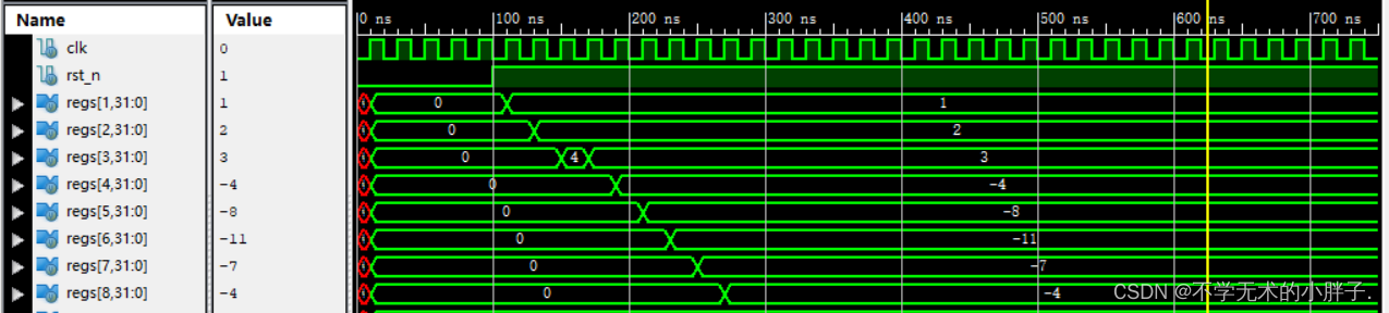
The arithmetic operation instructions are as follows:
addi x1,x0,1
add x2,x1,x1
add x3,x2,x2
sub x3,x3,x1

addi x4,x0,-4
add x5,x4,x4
sub x6,x5,x3
sub x7,x6,x4
add x8,x7,x3
The execution result of the assembler is as follows:
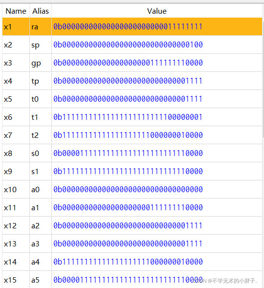
The CPU execution results are as follows:
The shift operation instructions are as follows:
addi x1,x0,0xff
addi x2,x0,4
sll x3,x1,x2
srl x4,x1,x2
sra x5,x1,x2

addi x6,x0,-0xff
sll x7,x6,x2
srl x8,x6,x2
sra x9,x6,x2

slli x11,x1,4
srli x12,x1,4
srai x13,x1,4

slli x11,x6,4
srli x12,x6,4
srai x13,x6,4
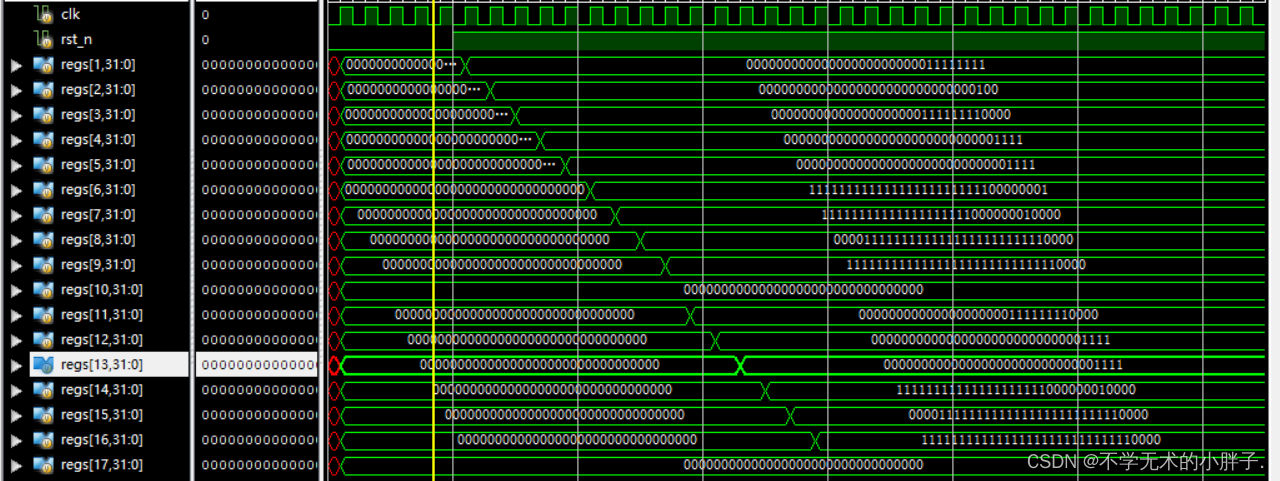
The execution result of the assembler is as follows:

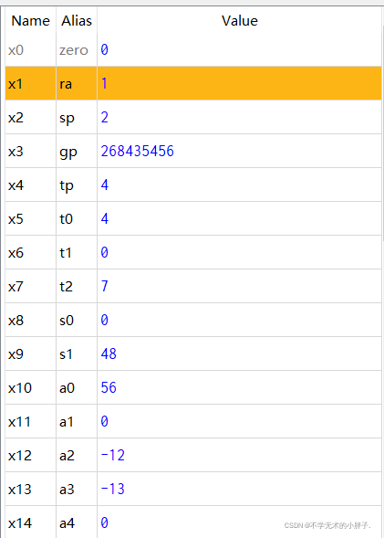
The CPU execution results are as follows:
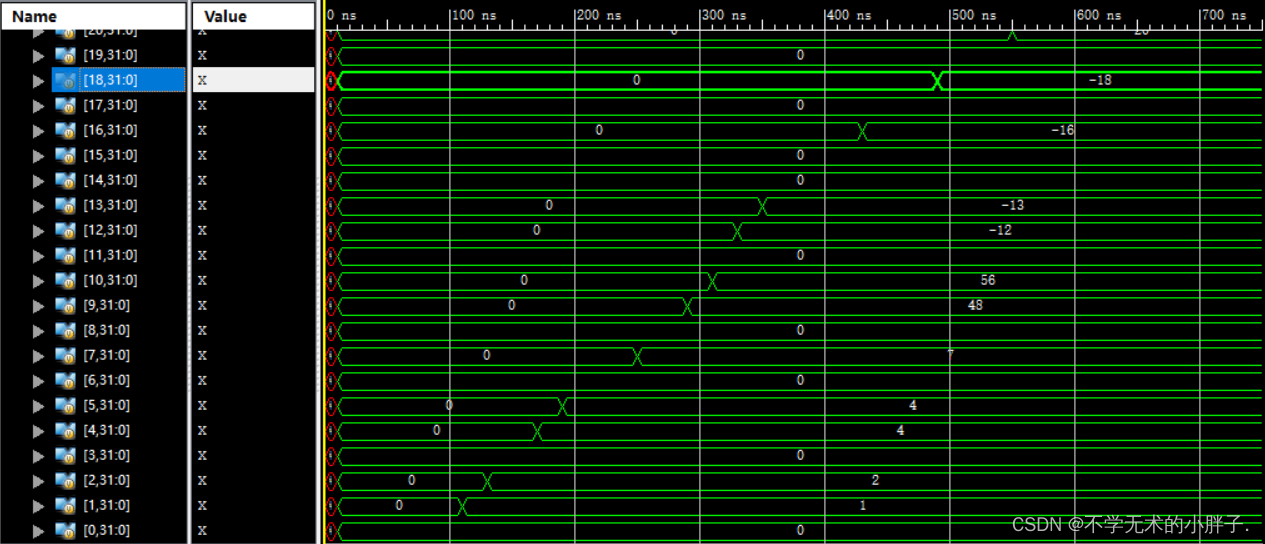
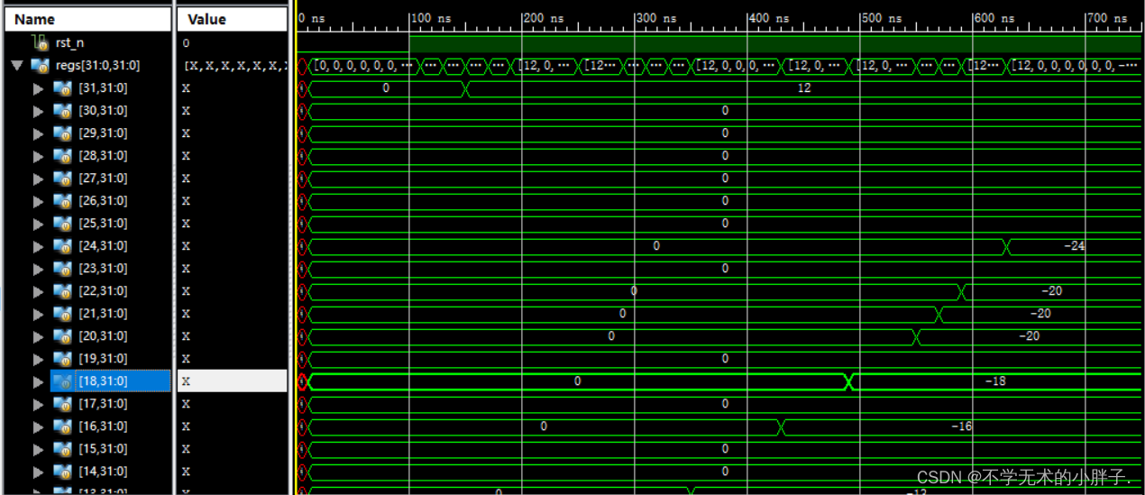
The jump instructions are as follows:
addi x1,x0,1
addi x2,x0,2
jal x31,label1
addi x3,x0,3
label1:
addi x4,x0,4
add x5,x2,x2
beq x4,x5,label2
addi x6,x0,6
label2:
bne x4,x5,label3
addi x7,x0,7
label3:
bne x7,x6,label4
addi x8,x0,8
label4:
addi x9,x0,0x30
jalr x10,x9,12
addi x11,x0,11
addi x12,x0,-12
addi x13,x0,-13
blt x13,x12,label5
addi x14,x0,-14
label5:
bltu x13,x12,label6
addi x15,x0,-15
label6:
bltu x12,x13,label7
addi x16,x0,-16
label7:
bge x12,x13,label8
addi x17,x0,-17
label8:
bge x1,x2,label9
addi x18,x0,-18
label9:
bgeu x12,x13,label10
addi x19,x0,-19
label10:
bgeu x13,x12,label11
addi x20,x0,-20
label11:
addi x21,x0,-20
addi x22,x0,-20
bge x21,x22,label12
addi x23,x0,-23
label12:
addi x24,x0,-24
The execution result of the assembler is as follows:
The CPU execution results are as follows: