Experiment Name: electronic organ design - task 2
(for learning purposes only, please indicate the source)
1, Experimental circuit diagram, state diagram, flow chart, program code, simulation code and simulation waveform diagram (only core function code can be written, and the code shall be annotated)
1. Design idea
Selections:
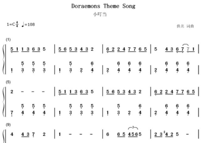
The design based on task 1 only needs to redesign the part that controls the duration of notes. Read the brief score of this music and know that the shortest note is an eighth note, the quarter note is a beat, four beats per section, 60s/108 ≈ 0.5s per beat. Only a 4hz clock is needed to generate the duration of an eighth note, and other notes are integer multiples of 0.25s (the duration of an eighth note in this song). You only need to record the corresponding times when recording the spectrum. For example, for a quarter note, you need to remember the sound name twice.
The realization of score recording adopts the idea in the experimental requirements: "the automatic playback function needs to write a" data table "(which can be a register array or a case statement) in the code, and the data table stores the frequency division coefficient corresponding to each note of the score.", which is realized by case statement.
In order to realize circular playback, it is necessary to design a counter, send the corresponding frequency division coefficient to the frequency divider when recording the corresponding number, and count again from 0 when recording the last note, so as to achieve the goal of circular playback.
2. Program code
module lyj_3501_7(mode_change,clk_in,clr,key,clk_out,clk_out_1,seg,codeout,beat);
//Preset frequency division ratio
parameter  O=14'd0;//Rest
parameter DO_=14'd11468;//Alto 1
parameter RE_=14'd10215;//Alto 2
parameter MI_=14'd9102;//Alto 3
parameter FA_=14'd8591;//Alto 4
parameter SO_=14'd7653;//Alto 5
parameter LA_=14'd6818;//Alto 6
parameter SI_=14'd6073;//Alto 7

parameter DO=14'd5736;//Treble 1
parameter RE=14'd5111;//Treble 2
parameter MI=14'd4552;//Treble 3
parameter FA=14'd4289;//Treble 4
parameter SO=14'd3827;//Treble 5
parameter LA=14'd3409;//Treble 6
parameter SI=14'd3037;//Treble 7
//input
input mode_change;
input [13:0]key;//14 key inputs
input clk_in;//The clock is 6Mhz
input clr;//Reset signal
//Test signal convenient for simulation
output beat;
//output
output reg clk_out;//Frequency divider signal output
output clk_out_1;//And clk_out consistent
output [7:0] codeout;//Eight segment nixie tube
output seg;//Nixie tube position selection signal
//Internal variable
reg [13:0]divider;//division factor
reg [13:0]cnt;//Counter
reg flag;

//Task 2 internal variables
reg [19:0] cnt_clk_4hz;//4hz counter
reg clk_4hz;//Half shot 0.25s, one shot 0.5s
reg [7:0] beat;//Timing, looping
reg [13:0]divider_;//division factor
assign clk_out_1=clk_out;//And clk_out consistent

//Get a clock of 4hz
always@(posedge clk_in or posedge clr)
begin
	if(clr)
	begin
			clk_4hz<=0;
			cnt_clk_4hz<=0;
	end
	else
	begin
			if(cnt_clk_4hz<750_000)
				cnt_clk_4hz<=cnt_clk_4hz+1'b1;
			else
			begin
				clk_4hz<=~clk_4hz;
				cnt_clk_4hz<=0;
			end
	end
end

//Frequency divider
always@(posedge clk_in or posedge clr)
begin
		if(clr)//Asynchronous reset, high level active
		begin
				flag<=1;
				cnt<=0;
		end
		else
		begin
			if(mode_change==0)
			begin
					if(cnt<divider)
					begin
							cnt<=cnt+1'b1;
							flag<=1'b0;
					end
					else
					begin
							flag<=1'b1;
							cnt<=1'b0;
					end
			end
			else
			begin
					if(cnt<divider_)
					begin
							cnt<=cnt+1'b1;
							flag<=1'b0;
					end
					else
					begin
							flag<=1'b1;
							cnt<=1'b0;
					end
			end
		end
end

//Waveform generation
always@(posedge flag)
begin//flag==1 indicates that the count is full, and the waveform is reversed
	if(clr)
	begin
		clk_out<=0;
	end
	else
		begin
				if(key!=0||mode_change==1)
					clk_out<=~clk_out;//The square wave signal with 50% duty cycle is obtained
				else
					clk_out<=1'd0;
		end
end

always@(key)
begin
		case(key)//Preset the frequency division ratio according to different notes
			14'b0000_000_0000_000:divider<=0;
			14'b1000_000_0000_000:divider<=14'd11468;
			14'b0100_000_0000_000:divider<=14'd10215;
			14'b0010_000_0000_000:divider<=14'd9102;
			14'b0001_000_0000_000:divider<=14'd8591;
			14'b0000_100_0000_000:divider<=14'd7653;
			14'b0000_010_0000_000:divider<=14'd6818;
			14'b0000_001_0000_000:divider<=14'd6073;
			14'b0000_000_1000_000:divider<=14'd5736;
			14'b0000_000_0100_000:divider<=14'd5111;
			14'b0000_000_0010_000:divider<=14'd4552;
			14'b0000_000_0001_000:divider<=14'd4289;
			14'b0000_000_0000_100:divider<=14'd3827;
			14'b0000_000_0000_010:divider<=14'd3409;
			14'b0000_000_0000_001:divider<=14'd3037;
			default:divider<=0;
		endcase
end

always@(posedge clk_4hz)
begin
	if(mode_change==1)
	begin
			if(beat==8'd72)
				beat<=8'd0;
			else
				beat<=beat+1'b1;
	end
	else
	begin
			beat<=0;
	end
	case(beat)//Notation (tinkle Bell)
				0	:divider_<=O;    //Rest
				1	:divider_<=SO_;	41	:divider_<=SO_;
				2	:divider_<=DO;		42	:divider_<=DO;
				3	:divider_<=DO;		43	:divider_<=DO;
				4	:divider_<=MI;		44	:divider_<=MI;
				5	:divider_<=LA;		45	:divider_<=LA;
				6	:divider_<=MI;		46	:divider_<=MI;
				7	:divider_<=SO;		47	:divider_<=SO;
				8	:divider_<=SO;		48	:divider_<=SO;
				//Section 1 / / section 6
				9	:divider_<=SO;		49	:divider_<=SO;
				10	:divider_<=LA;		50	:divider_<=LA;
				11	:divider_<=SO;		51	:divider_<=SO;
				12	:divider_<=MI;		52	:divider_<=MI;
				13	:divider_<=FA;		53	:divider_<=FA;
				14	:divider_<=MI;		54	:divider_<=MI;
				15	:divider_<=RE;		55	:divider_<=RE;
				16	:divider_<=RE;		56	:divider_<=RE;
				//Section II / / Section VII
				17	:divider_<=LA_;		57	:divider_<=LA_;
				18	:divider_<=RE;		58	:divider_<=RE;
				19	:divider_<=RE;		59	:divider_<=RE;
				20	:divider_<=FA;		60	:divider_<=FA;
				21	:divider_<=SI;		61	:divider_<=SI;
				22	:divider_<=SI;		62	:divider_<=SI;
				23	:divider_<=LA;		63	:divider_<=LA;
				24	:divider_<=SO;		64	:divider_<=SO;
				// Section III / / Section VIII
				25	:divider_<=SO;		65	:divider_<=FA;
				26	:divider_<=SO;		66	:divider_<=FA;
				27	:divider_<=FA;		67	:divider_<=FA;
				28	:divider_<=MI;		68	:divider_<=MI;
				29	:divider_<=LA_;	69	:divider_<=SI_;
				30	:divider_<=SI_;	70	:divider_<=SI_;
				31	:divider_<=SI_;	71	:divider_<=RE;
				32	:divider_<=DO;		72	:divider_<=RE;
				// Section 5 / / section 9
				33	:divider_<=RE;
				34	:divider_<=RE;
				35	:divider_<=RE;
				36	:divider_<=RE;
				37	:divider_<=RE;
				38	:divider_<=O ;
				39	:divider_<=O ;
				40	:divider_<=O ;
				//Section VI
				default:divider_<=O;//Rest
			endcase
end
lyj_3501_6_b u1(key,codeout,seg);
endmodule

module lyj_3501_6_b(key,codeout,seg);//Decoder module
input [13:0] key;
output reg[7:0] codeout;
output seg;

assign seg=1'b1;//Nixie tube position selection signal

always@ (key)
begin
	case(key)
	14'b1000_000_0000_000:codeout=8'b0_0000110;//Alto 1
	14'b0100_000_0000_000:codeout=8'b0_1011011;//Alto 2
	14'b0010_000_0000_000:codeout=8'b0_1001111;//Alto 3
	14'b0001_000_0000_000:codeout=8'b0_1100110;//Alto 4
	14'b0000_100_0000_000:codeout=8'b0_1101101;//Alto 5
	14'b0000_010_0000_000:codeout=8'b0_1111101;//Alto 6
	14'b0000_001_0000_000:codeout=8'b0_0000111;//Alto 7

	14'b0000_000_1000_000:codeout=8'b1_0000110;//Treble 1
	14'b0000_000_0100_000:codeout=8'b1_1011011;//Treble 2
	14'b0000_000_0010_000:codeout=8'b1_1001111;//Treble 3
	14'b0000_000_0001_000:codeout=8'b1_1100110;//Treble 4
	14'b0000_000_0000_100:codeout=8'b1_1101101;//Treble 5
	14'b0000_000_0000_010:codeout=8'b1_1111101;//Treble 6
	14'b0000_000_0000_001:codeout=8'b1_0000111;//Treble 7

	14'b0000_000_0000_000:codeout=8'b1_1111111;//Rest
	              default:codeout=8'b1_0111111;//0
	endcase
end
endmodule
//Test file
`timescale 1ns / 1ns//Time unit / time precision
module test_lyj_3501_7;
reg clk_in,clr;
reg [13:0]key;
reg mode_change;

wire [7:0]beat;//It is convenient to observe the simulation results
wire seg;
wire [7:0]codeout;
wire clk_out_1,clk_out;

lyj_3501_7 test_a(.mode_change(mode_change),.clk_in(clk_in),.clr(clr),.key(key),.clk_out(clk_out),.clk_out_1(clk_out_1),.seg(seg),.codeout(codeout),.beat(beat));

always #83 clk_in=~clk_in;// Clock approximately 6Mhz

initial
begin
	clk_in=1'b0;
	clr=1'b1;
	key=14'd0;
	#1000
	clr=1'b0;
	#1000
	mode_change=0;
	#1_000_000_000
	mode_change=1;
end
endmodule
3. Simulation waveform
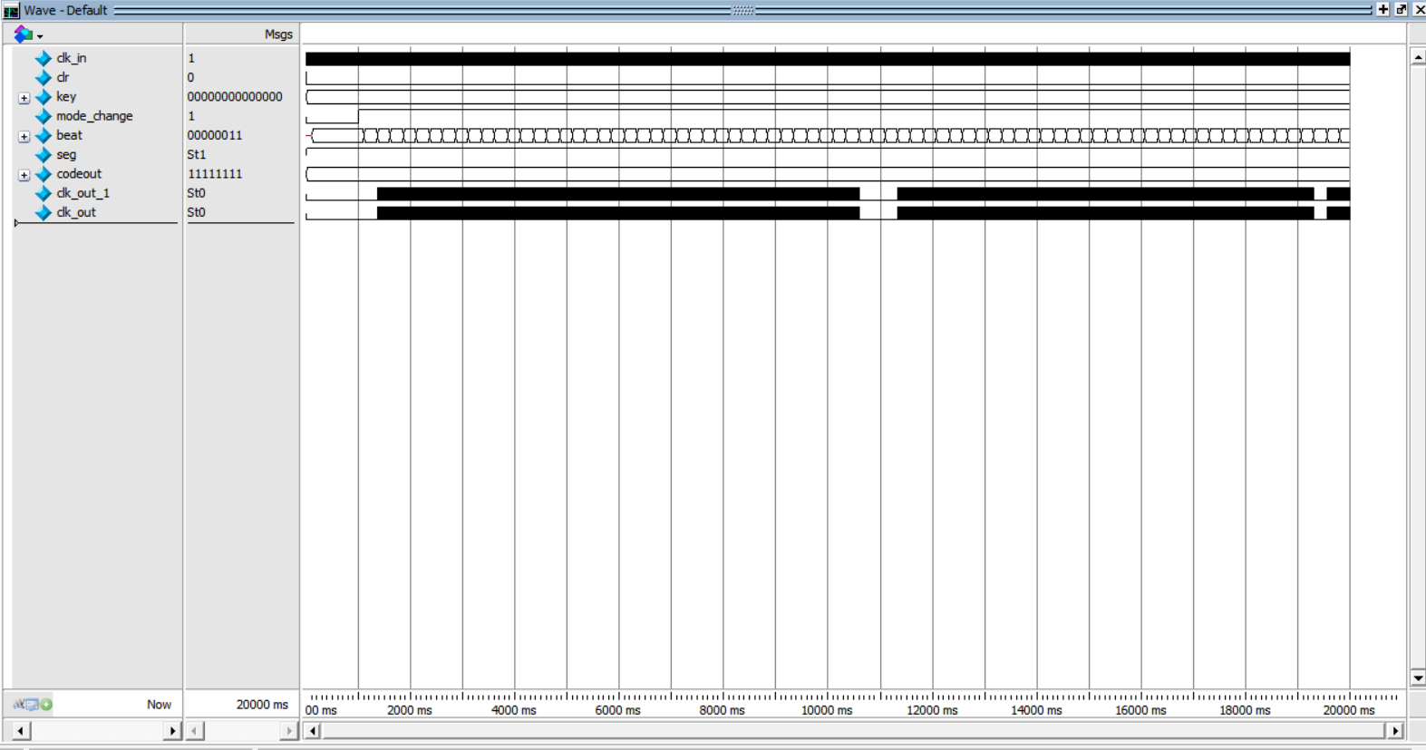
There are too many data, and the error analysis has been done in task 1, and the random sampling results also meet the requirements
Frequency: 393.52HZ
2, PIN assignment table (signal name in circuit - > mainboard device name - > PIN number PIN)
Signal name motherboard device PIN signal name motherboard device PIN
key[13] Key13 PIN_7 codeout[0] a PIN_112
key[12] Key12 PIN_8 codeout[1] b PIN_100
key[11] Key11 PIN_144 codeout[2] c PIN_104
key[10] Key10 PIN_6 codeout[3] d PIN_111
key[9] Key9 PIN_13 codeout[4] e PIN_106
key[8] Key8 PIN_43 codeout[5] f PIN_110
key[7] Key7 PIN_44 codeout[6] g PIN_103
key[6] Key6 PIN_39 codeout[7] h PIN_105
key[5] Key5 PIN_42 seg SEG0 PIN_119
key[4] Key4 PIN_32 clk_out speaker pin_ one hundred and twenty-eight
key[3] Key3 PIN_33 clk_out_1 LED0/IO0 PIN_46
key[2] Key2 PIN_30 mode_change Key16 PIN_142
key[1] Key1 PIN_31
key[0] Key0 PIN_24
clk_in Clk0 PIN_88
clr Key17 PIN_137
3, Experimental phenomena and original data records
Top-level Entity name Family Device
lyj_3501_7 Cyclone IV E EP4CE6E22C8
Total logic elements Total registers Total pins
265 45 37
Total memory bits Embedded Multiplier 9-bit elements Total PLLs
0 0 0
Waveform diagram and truth table
reference material:
Wang Jinming, Xu Zhijun, Su Yong. EDA technology and Verilog HDL design [M]: Electronic Industry Press, 2013