Article catalog
Experiment 1: project creation, compilation and download
Experiment 2: FPGA decoder combinational logic
Experiment 3: counter waveform simulation and signalTap
Experiment 4: time reference circuit and multi period counter with Enable
Experiment 5: multi cycle shift register circuit
Experiment 6: counter, ROM and DDS
Experiment 1: project creation, compilation and download
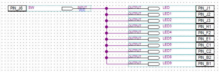
Experiment content: design a programmable wire and use a dial switch to control all LED lights on and off
Create a new bdf file, put 1 input pin, and then put 10 output pins to connect with input.
RTL diagram:
Refer to the pin correspondence in the DE0 manual, assign pins, compile and download.
Experiment 2: FPGA decoder combinational logic
1.2 2 2-4 decoder control LED s
1. Write 2-4 decoder with Verilog:
module dec_2to4(
IN  ,
OUT);
input  [2-1:0] IN  ;
output [4-1:0] OUT ;
reg [4-1:0] OUT ;

always @ (IN) begin
  case(IN)
    2'b00: OUT = 4'b 0001;
    2'b01: OUT = 4'b 0010;
    2'b10: OUT = 4'b 0100;
    2'b11: OUT = 4'b 1000;
  endcase
end

endmodule // module dec_2to4;
2. create symbol for code file (symbol) for calling in bdf file.
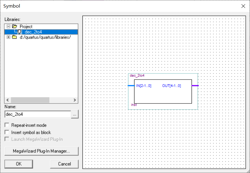
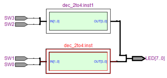
3. Put in input and output, connect and assign pins
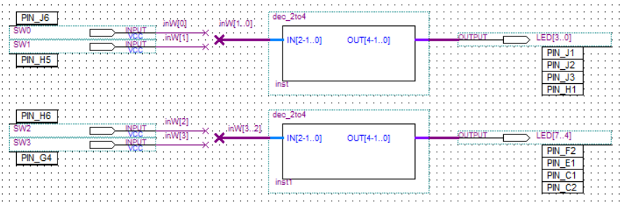 RTL diagram:
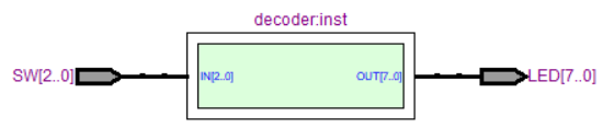
2.1 3-8 decoder control LED s
1. Write 3-8 decoder with Verilog:
module decoder(
IN,
OUT
);
input [2:0]IN;
output [7:0]OUT;
reg [7:0]OUT;

always @ (IN) begin
	case(IN)
		3'b000: OUT = 8'b00000001;
		3'b001: OUT = 8'b00000010;
		3'b010: OUT = 8'b00000100;
		3'b011: OUT = 8'b00001000;
		3'b100: OUT = 8'b00010000;
		3'b101: OUT = 8'b00100000;
		3'b110: OUT = 8'b01000000;
		3'b111: OUT = 8'b10000000;
	endcase
end

endmodule
2. create symbol for code file (symbol) for calling in bdf file.
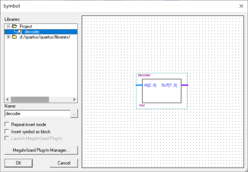
3. Put in input and output, connect, assign pins, compile and download.
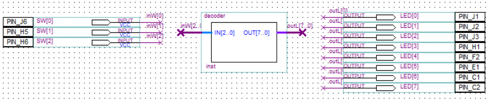
RTL diagram:
3.4 dial switches control 7-segment nixie tubes
1. Write 4-7 decoder with Verilog:
module dec4_7(
IN,
OUT);

input [3:0]IN;
output [6:0]OUT;
reg [6:0]OUT;

always @ (IN) begin
	case(IN)
		4'b0000: OUT = 7'b1000000;
		4'b0001: OUT = 7'b1111001;
		4'b0010: OUT = 7'b0100100;
		4'b0011: OUT = 7'b0110000;

		4'b0100: OUT = 7'b0011001;
		4'b0101: OUT = 7'b0010010;
		4'b0110: OUT = 7'b0000010;
		4'b0111: OUT = 7'b1111000;

		4'b1000: OUT = 7'b0000000;
		4'b1001: OUT = 7'b0010000;
		4'b1010: OUT = 7'b0001000;
		4'b1011: OUT = 7'b0000011;

		4'b1100: OUT = 7'b1000110;
		4'b1101: OUT = 7'b0100001;
		4'b1110: OUT = 7'b0000110;
		4'b1111: OUT = 7'b0001110;
	endcase
end

endmodule
2. create symbol for code file (symbol) for calling in bdf file.
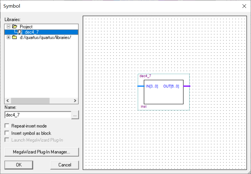
3. Put in input and output, connect and assign pins
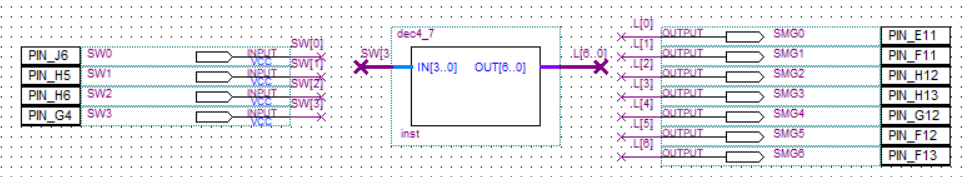
RTL diagram:
Experiment 3: counter waveform simulation and signalTap
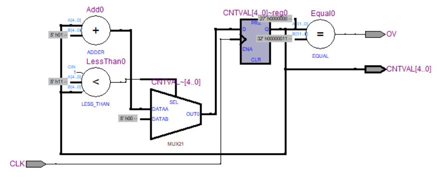
1. Design a 0-17 counter
1. Write out the 0-17 counter with Verilog and generate a symbol
module cnt_0to17(
  CLK   ,   // clock
  CNTVAL,   // counter value
  OV    );  // overflow
input CLK;
output [4:0] CNTVAL;
output OV;

reg [4:0] CNTVAL;
reg OV;

always @ (posedge CLK) begin
  if(CNTVAL >= 17)
    CNTVAL <= 0;
  else
    CNTVAL <= CNTVAL + 1'b1;
end

always @ (CNTVAL) begin
  if(CNTVAL == 17)
    OV = 1'b1;
  else
    OV = 1'b0;
end

endmodule   // module cnt_0to17
2. Create bdf file, connect, compile
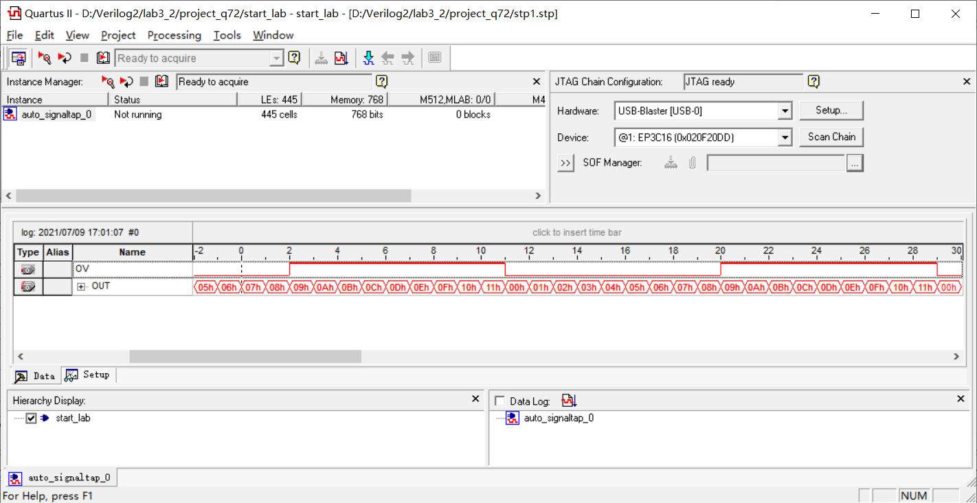
3. Verify with SignalTap
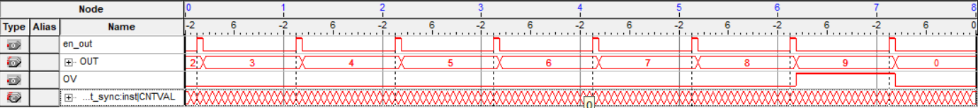
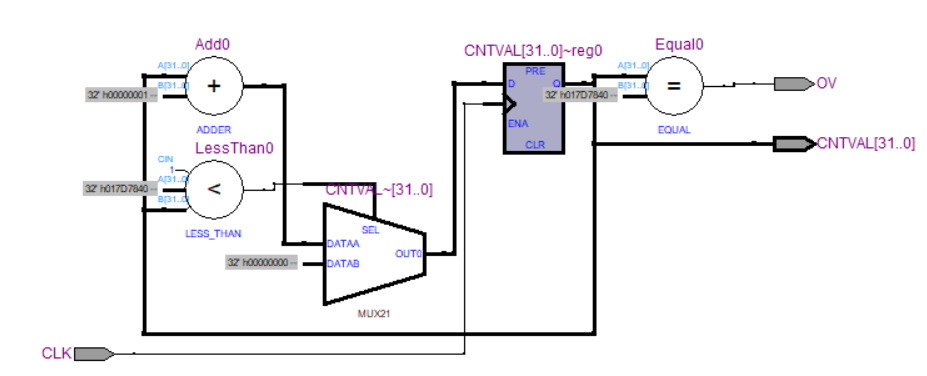
As shown in the figure, the range of the counter is 0-17, and OV is 1 every 17 to 17.
RTL diagram:
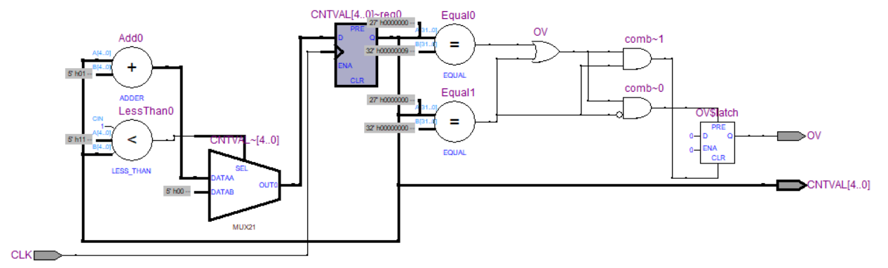
2. Modify 0-17 counter
Requirements: modify the output logic. When the count value is 0-8, OV outputs 0, and when 9-17, OV outputs 1
1. Modify the 0-17 counter and generate a symbol
module cnt_0to17(
  CLK   ,   // clock
  CNTVAL,   // counter value
  OV    );  // overflow
input CLK;
output [4:0] CNTVAL;
output OV;

reg [4:0] CNTVAL;
reg OV;

always @ (posedge CLK) begin
  if(CNTVAL >= 17)
    CNTVAL <= 0;
  else
    CNTVAL <= CNTVAL + 1'b1;
end

always @ (CNTVAL) begin
  if(CNTVAL == 9)
    OV = 1'b1;
  if(CNTVAL == 0)
    OV = 1'b0;
end

endmodule   // module cnt_0to17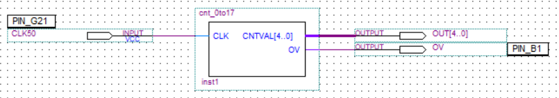
2. Verify with SignalTap that the OV is 0 at 0-8 and 1 at 9-17
The phenomenon of connecting the OV of two counters to the LED: the brightness of the first counter LED is very dark, and the brightness of the second counter LED is brighter. The duty cycle of the OV affects the enabling time of the LED, and then affects the brightness of the LED.
RTL diagram:
Experiment 4: time reference circuit and multi period counter with Enable
Requirements: 1 Design time reference circuit and multi period counter with enable
2. The time reference circuit generates a synchronous time reference signal
3. The multi cycle counter counts the time reference signal
4. It is essentially a two-stage counter cascade circuit structure: the first stage counter generates a time reference signal, and the second stage counter uses the time reference signal as the count enable
1. Counter
Requirement: the counting range of the subsequent counter is 0-15. The 0-15 count value of the counter is decoded and displayed as a hexadecimal number of 0-9-A-F on the HEX LED of DE0
Two counters: and generate symbol
module cnt_sync(
  CLK   ,   // clock
  CNTVAL,   // counter value
  OV    );  // overflow
input CLK;
output [32-1:0] CNTVAL;
output OV;
parameter MAX_VAL = 25_000_000;
reg [32-1:0] CNTVAL;
reg OV;

always @ (posedge CLK) begin
  if(CNTVAL >= MAX_VAL)
    CNTVAL <= 0;
  else
    CNTVAL <= CNTVAL + 1'b1;
end

always @ (CNTVAL) begin
  if(CNTVAL == MAX_VAL)
    OV = 1'b1;
  else
    OV = 1'b0;
end

endmodule   // module cnt_sync
module cnt_en_0to15(
CLK , // clock
CNTVAL, // counter value
EN ,
SMG ,
OV ); // overflow
input CLK;
input EN;
output [4-1:0] CNTVAL;
output OV;
output [7-1:0] SMG;
reg [4-1:0] CNTVAL;
reg OV;
reg [7-1:0] SMG;
always @ (posedge CLK) begin
if(EN) begin // work enable
if(CNTVAL >= 15)
CNTVAL <= 0;
else
CNTVAL <= CNTVAL + 1'b1;
end
else
CNTVAL <= CNTVAL ; // hold same value
end
always @ (CNTVAL) begin
if(CNTVAL == 15)
OV = 1'b1;
else
OV = 1'b0;
end
always @ (CNTVAL)begin
case(CNTVAL)
4'b0000: SMG = 7'b1000000;
4'b0001: SMG = 7'b1111001;
4'b0010: SMG = 7'b0100100;
4'b0011: SMG = 7'b0110000;
4'b0100: SMG = 7'b0011001;
4'b0101: SMG = 7'b0010010;
4'b0110: SMG = 7'b0000010;
4'b0111: SMG = 7'b1111000;
4'b1000: SMG = 7'b0000000;
4'b1001: SMG = 7'b0010000;
4'b1010: SMG = 7'b0001000;
4'b1011: SMG = 7'b0000011;
4'b1100: SMG = 7'b1000110;
4'b1101: SMG = 7'b0100001;
4'b1110: SMG = 7'b0000110;
4'b1111: SMG = 7'b0001110;
endcase
end
endmodule // module cnt_en_0to15Connect and verify with SignalTap
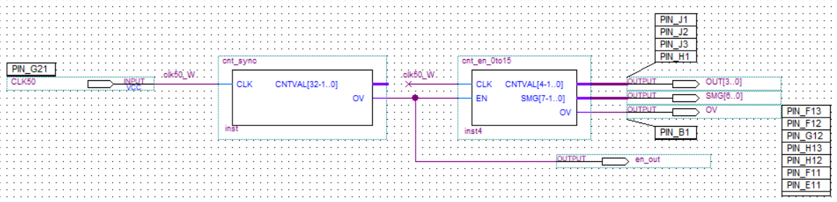
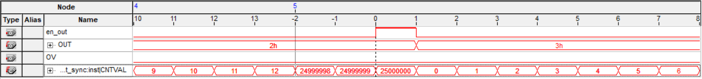
Zoom out:
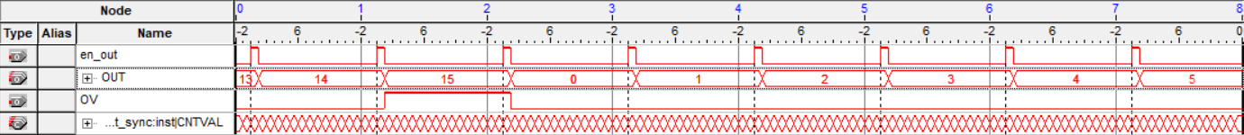
As shown in the figure, the range of the former counter is 0-25000000, en is 1 every time to 25000000, and the range of the latter counter is 0-15, OV is 1 every 15.
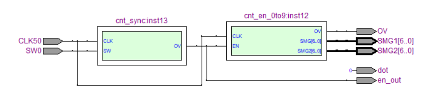
2. Timing stopwatch with a range of 0-9.9 seconds (with pause function)
Two stage counter, the latter stage with 4-7 decoding:
module cnt_sync(
  CLK   ,   // clock
  SW    ,
  CNTVAL,   // counter value
  OV    );  // overflow
input CLK;
input SW;
output [32-1:0] CNTVAL;
output OV;
parameter MAX_VAL = 5_000_000;
reg [32-1:0] CNTVAL;
reg OV;

always @ (posedge CLK) begin
	if(SW ==1)begin
		if(CNTVAL >= MAX_VAL)
			CNTVAL <= 0;
		else
			CNTVAL <= CNTVAL + 1'b1;
	end
end

always @ (CNTVAL) begin
  if(CNTVAL == MAX_VAL)
    OV = 1'b1;
  else
    OV = 1'b0;
end

endmodule   // module cnt_sync

module cnt_en_0to9(
  CLK   ,   // clock
  EN    ,
  SMG,SMG2,
  OV    );  // overflow
input CLK;
input EN;
output OV;
output [7-1:0] SMG;
output [7-1:0] SMG2;

reg [4-1:0] CNTVAL;
reg [4-1:0] CNT;
reg OV;
reg [7-1:0] SMG;
reg [7-1:0] SMG2;

always @ (posedge CLK) begin
  if(EN) begin  // work enable
    if(CNTVAL >= 9)
      CNTVAL <= 0;
    else
      CNTVAL <= CNTVAL + 1'b1;
  end
  else
    CNTVAL <= CNTVAL ;  // hold same value
end

always @ (CNTVAL) begin
  if(CNTVAL == 9)
    OV = 1'b1;
  else
    OV = 1'b0;
end

always @ (negedge OV) begin
	if(CNT >= 9)
		CNT <= 0;
	else
		CNT <= CNT + 1'b1;
end

always @ (CNTVAL) begin
	case(CNTVAL)
		4'b0000: SMG = 7'b1000000;
		4'b0001: SMG = 7'b1111001;
		4'b0010: SMG = 7'b0100100;
		4'b0011: SMG = 7'b0110000;
		4'b0100: SMG = 7'b0011001;

		4'b0101: SMG = 7'b0010010;
		4'b0110: SMG = 7'b0000010;
		4'b0111: SMG = 7'b1111000;
		4'b1000: SMG = 7'b0000000;
		4'b1001: SMG = 7'b0010000;
	endcase
end

always @ (CNT) begin
	case(CNT)
		4'b0000: SMG2 = 7'b1000000;
		4'b0001: SMG2 = 7'b1111001;
		4'b0010: SMG2 = 7'b0100100;
		4'b0011: SMG2 = 7'b0110000;
		4'b0100: SMG2 = 7'b0011001;

		4'b0101: SMG2 = 7'b0010010;
		4'b0110: SMG2 = 7'b0000010;
		4'b0111: SMG2 = 7'b1111000;
		4'b1000: SMG2 = 7'b0000000;
		4'b1001: SMG2 = 7'b0010000;
	endcase
end

endmodule   // module cnt_en_0to9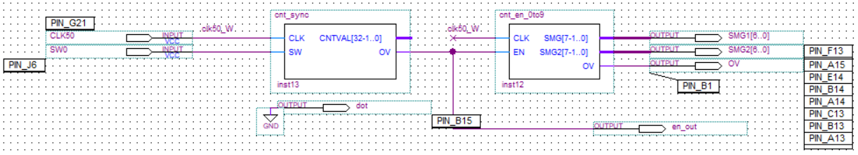
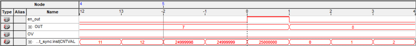
Verify with SignalTap: the range of the former counter is changed to 0-5000000, and enable the latter counter, and the range of the latter counter is changed to 0-9.
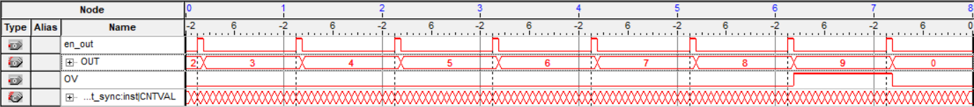
RTL diagram:
Experiment 5: multi cycle shift register circuit
Effect: shift the status value of a dial switch into the lowest position of the register, move the value of the shift register in sequence, and send each bit of the register to an LED lamp for display
Requirements: SW1 can control the movement direction of LED flashing and the input position of SW0 value to LED group (i.e. from the leftmost or rightmost of LED group)
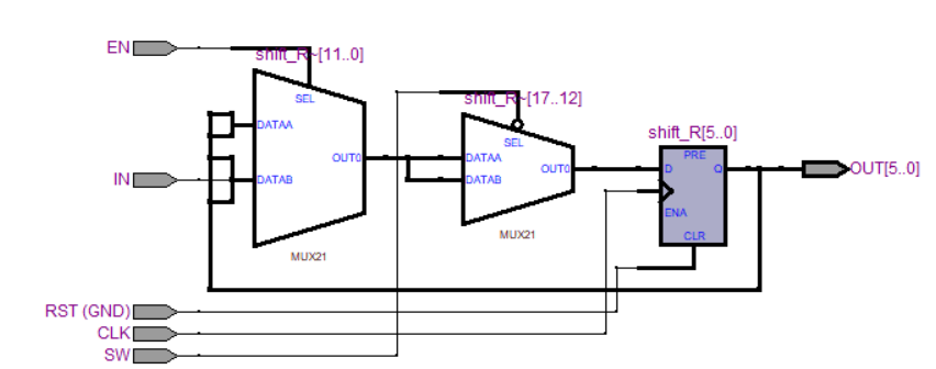
 Serial in parallel out shift register  /
module shift_reg_SIPO(
  RST   ,   // Asynchronous reset, high effective
  CLK   ,   // Clock, rising edge valid
  EN    ,   // Input data serial shift enable
  SW    ,   // Move left move right
  IN    ,   // Input serial data
  OUT   );  // Parallel output data
parameter SHLEN = 6;
input RST, CLK, EN, SW;
input IN;
output[SHLEN-1:0] OUT;
reg [SHLEN-1:0] shift_R;

assign OUT[SHLEN-1:0] = shift_R[SHLEN-1:0];
// The sequential logic performs a serial shift according to the input enable
// shift_R is compiled as a D trigger
always @ (posedge CLK or posedge RST) begin
	if(RST)
		shift_R[SHLEN-1:0] <= 0;
	else begin
		if(SW == 0)begin
			if(EN) begin // Serial shift enable effective
				shift_R[SHLEN-1:1] <= shift_R[SHLEN-2:0];
				shift_R[0]   <= IN;
			end
			else begin // Enable invalid hold
				shift_R[SHLEN-1:0] <= shift_R[SHLEN-1:0];
			end
		end
		else begin
			if(EN) begin // Serial shift enable effective
				shift_R[SHLEN-2:0] <= shift_R[SHLEN-1:1];
				shift_R[SHLEN-1]   <= IN;
			end
			else begin // Enable invalid hold
				shift_R[SHLEN-1:0] <= shift_R[SHLEN-1:0];
			end
		end
	end
end // always
endmodule

 Time reference counter  /
module cnt_sync(
  CLK   ,   // clock
  CNTVAL,   // counter value
  OV    );  // overflow
input CLK;
output [32-1:0] CNTVAL;
output OV;
parameter MAX_VAL = 25_000_000;
reg [32-1:0] CNTVAL;
reg OV;

always @ (posedge CLK) begin
  if(CNTVAL >= MAX_VAL)
    CNTVAL <= 0;
  else
    CNTVAL <= CNTVAL + 1'b1;
end

always @ (CNTVAL) begin
  if(CNTVAL == MAX_VAL)
    OV = 1'b1;
  else
    OV = 1'b0;
end

endmodule   // module cnt_sync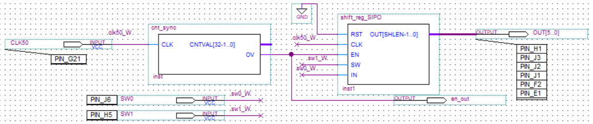
Verify with SignalTap:
RTL diagram:
Experiment 6: counter, ROM and DDS
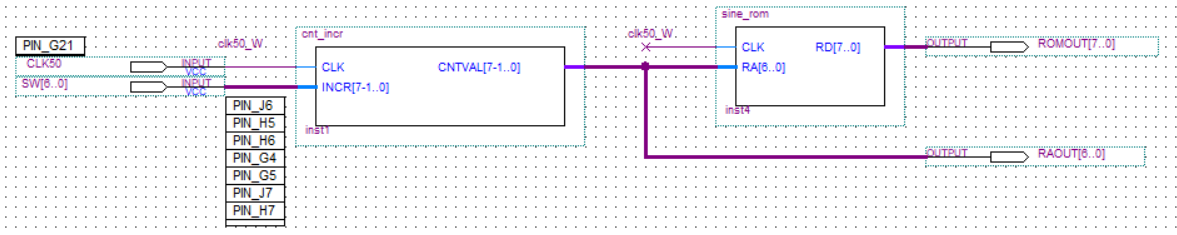
1. The working clock of the circuit is fsys = 50MHz, and the counter and ROM address are 7 bits:
Observe the output waveform with SignalTap:
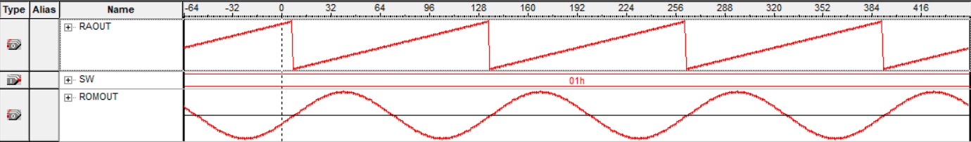
By adjusting the increment value of the counter, the frequency of the output waveform can be changed. Set the output sine wave frequency as f1, the circuit system clock as fsys, and the step increment of the counter as CNT
The formula is f1=fsys*CNT/128
The minimum frequency of output waveform is 50000000 * 1 / 128 = 390625hz
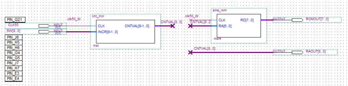
2. Modify the circuit to change the count value of the counter and the input count increment signal to 9 bits. The upper 7 bits of the count value are connected to the address line of ROM, and the lower 2 bits are suspended.
Observe the output waveform with SignalTap:
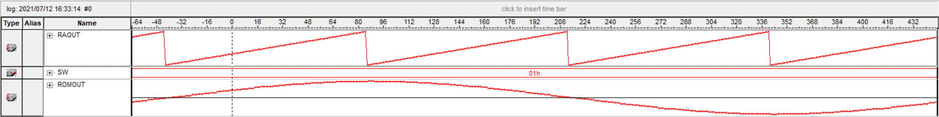
By adjusting the increment value of the counter, the frequency of the output waveform can be changed. Set the output sine wave frequency as f1, the circuit system clock as fsys, and the step increment of the counter as CNT
The formula is f1=fsys*CNT / (128 * 4)
The lowest frequency of output waveform is 390625 / 4 = 97656.25hz
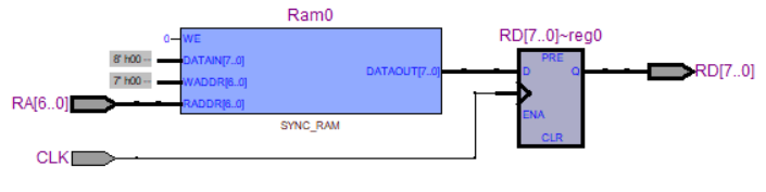
verilog code of the above two modules:
module sine_rom(
CLK , // clock
RA , // read address
RD ); // read data
input CLK;
input [6 :0] RA;
output [7 :0] RD;
reg [7 :0] RD;
always @ (posedge CLK)
case(RA)
7 'd 0 :RD = #1 8 'b 00000000; // 0 0x0
7 'd 1 :RD = #1 8 'b 00000110; // 6 0x6
7 'd 2 :RD = #1 8 'b 00001100; // 12 0xC
7 'd 3 :RD = #1 8 'b 00010010; // 18 0x12
7 'd 4 :RD = #1 8 'b 00011000; // 24 0x18
7 'd 5 :RD = #1 8 'b 00011110; // 30 0x1E
7 'd 6 :RD = #1 8 'b 00100100; // 36 0x24
7 'd 7 :RD = #1 8 'b 00101010; // 42 0x2A
7 'd 8 :RD = #1 8 'b 00110000; // 48 0x30
7 'd 9 :RD = #1 8 'b 00110110; // 54 0x36
7 'd 10 :RD = #1 8 'b 00111011; // 59 0x3B
7 'd 11 :RD = #1 8 'b 01000001; // 65 0x41
7 'd 12 :RD = #1 8 'b 01000110; // 70 0x46
7 'd 13 :RD = #1 8 'b 01001011; // 75 0x4B
7 'd 14 :RD = #1 8 'b 01010000; // 80 0x50
7 'd 15 :RD = #1 8 'b 01010101; // 85 0x55
7 'd 16 :RD = #1 8 'b 01011001; // 89 0x59
7 'd 17 :RD = #1 8 'b 01011110; // 94 0x5E
7 'd 18 :RD = #1 8 'b 01100010; // 98 0x62
7 'd 19 :RD = #1 8 'b 01100110; // 102 0x66
7 'd 20 :RD = #1 8 'b 01101001; // 105 0x69
7 'd 21 :RD = #1 8 'b 01101100; // 108 0x6C
7 'd 22 :RD = #1 8 'b 01110000; // 112 0x70
7 'd 23 :RD = #1 8 'b 01110010; // 114 0x72
7 'd 24 :RD = #1 8 'b 01110101; // 117 0x75
7 'd 25 :RD = #1 8 'b 01110111; // 119 0x77
7 'd 26 :RD = #1 8 'b 01111001; // 121 0x79
7 'd 27 :RD = #1 8 'b 01111011; // 123 0x7B
7 'd 28 :RD = #1 8 'b 01111100; // 124 0x7C
7 'd 29 :RD = #1 8 'b 01111101; // 125 0x7D
7 'd 30 :RD = #1 8 'b 01111110; // 126 0x7E
7 'd 31 :RD = #1 8 'b 01111110; // 126 0x7E
7 'd 32 :RD = #1 8 'b 01111111; // 127 0x7F
7 'd 33 :RD = #1 8 'b 01111110; // 126 0x7E
7 'd 34 :RD = #1 8 'b 01111110; // 126 0x7E
7 'd 35 :RD = #1 8 'b 01111101; // 125 0x7D
7 'd 36 :RD = #1 8 'b 01111100; // 124 0x7C
7 'd 37 :RD = #1 8 'b 01111011; // 123 0x7B
7 'd 38 :RD = #1 8 'b 01111001; // 121 0x79
7 'd 39 :RD = #1 8 'b 01110111; // 119 0x77
7 'd 40 :RD = #1 8 'b 01110101; // 117 0x75
7 'd 41 :RD = #1 8 'b 01110010; // 114 0x72
7 'd 42 :RD = #1 8 'b 01110000; // 112 0x70
7 'd 43 :RD = #1 8 'b 01101100; // 108 0x6C
7 'd 44 :RD = #1 8 'b 01101001; // 105 0x69
7 'd 45 :RD = #1 8 'b 01100110; // 102 0x66
7 'd 46 :RD = #1 8 'b 01100010; // 98 0x62
7 'd 47 :RD = #1 8 'b 01011110; // 94 0x5E
7 'd 48 :RD = #1 8 'b 01011001; // 89 0x59
7 'd 49 :RD = #1 8 'b 01010101; // 85 0x55
7 'd 50 :RD = #1 8 'b 01010000; // 80 0x50
7 'd 51 :RD = #1 8 'b 01001011; // 75 0x4B
7 'd 52 :RD = #1 8 'b 01000110; // 70 0x46
7 'd 53 :RD = #1 8 'b 01000001; // 65 0x41
7 'd 54 :RD = #1 8 'b 00111011; // 59 0x3B
7 'd 55 :RD = #1 8 'b 00110110; // 54 0x36
7 'd 56 :RD = #1 8 'b 00110000; // 48 0x30
7 'd 57 :RD = #1 8 'b 00101010; // 42 0x2A
7 'd 58 :RD = #1 8 'b 00100100; // 36 0x24
7 'd 59 :RD = #1 8 'b 00011110; // 30 0x1E
7 'd 60 :RD = #1 8 'b 00011000; // 24 0x18
7 'd 61 :RD = #1 8 'b 00010010; // 18 0x12
7 'd 62 :RD = #1 8 'b 00001100; // 12 0xC
7 'd 63 :RD = #1 8 'b 00000110; // 6 0x6
7 'd 64 :RD = #1 8 'b 00000000; // 0 0x0
7 'd 65 :RD = #1 8 'b 11111010; // -6 0xFA
7 'd 66 :RD = #1 8 'b 11110100; // -12 0xF4
7 'd 67 :RD = #1 8 'b 11101110; // -18 0xEE
7 'd 68 :RD = #1 8 'b 11101000; // -24 0xE8
7 'd 69 :RD = #1 8 'b 11100010; // -30 0xE2
7 'd 70 :RD = #1 8 'b 11011100; // -36 0xDC
7 'd 71 :RD = #1 8 'b 11010110; // -42 0xD6
7 'd 72 :RD = #1 8 'b 11010000; // -48 0xD0
7 'd 73 :RD = #1 8 'b 11001010; // -54 0xCA
7 'd 74 :RD = #1 8 'b 11000101; // -59 0xC5
7 'd 75 :RD = #1 8 'b 10111111; // -65 0xBF
7 'd 76 :RD = #1 8 'b 10111010; // -70 0xBA
7 'd 77 :RD = #1 8 'b 10110101; // -75 0xB5
7 'd 78 :RD = #1 8 'b 10110000; // -80 0xB0
7 'd 79 :RD = #1 8 'b 10101011; // -85 0xAB
7 'd 80 :RD = #1 8 'b 10100111; // -89 0xA7
7 'd 81 :RD = #1 8 'b 10100010; // -94 0xA2
7 'd 82 :RD = #1 8 'b 10011110; // -98 0x9E
7 'd 83 :RD = #1 8 'b 10011010; // -102 0x9A
7 'd 84 :RD = #1 8 'b 10010111; // -105 0x97
7 'd 85 :RD = #1 8 'b 10010100; // -108 0x94
7 'd 86 :RD = #1 8 'b 10010000; // -112 0x90
7 'd 87 :RD = #1 8 'b 10001110; // -114 0x8E
7 'd 88 :RD = #1 8 'b 10001011; // -117 0x8B
7 'd 89 :RD = #1 8 'b 10001001; // -119 0x89
7 'd 90 :RD = #1 8 'b 10000111; // -121 0x87
7 'd 91 :RD = #1 8 'b 10000101; // -123 0x85
7 'd 92 :RD = #1 8 'b 10000100; // -124 0x84
7 'd 93 :RD = #1 8 'b 10000011; // -125 0x83
7 'd 94 :RD = #1 8 'b 10000010; // -126 0x82
7 'd 95 :RD = #1 8 'b 10000010; // -126 0x82
7 'd 96 :RD = #1 8 'b 10000001; // -127 0x81
7 'd 97 :RD = #1 8 'b 10000010; // -126 0x82
7 'd 98 :RD = #1 8 'b 10000010; // -126 0x82
7 'd 99 :RD = #1 8 'b 10000011; // -125 0x83
7 'd 100 :RD = #1 8 'b 10000100; // -124 0x84
7 'd 101 :RD = #1 8 'b 10000101; // -123 0x85
7 'd 102 :RD = #1 8 'b 10000111; // -121 0x87
7 'd 103 :RD = #1 8 'b 10001001; // -119 0x89
7 'd 104 :RD = #1 8 'b 10001011; // -117 0x8B
7 'd 105 :RD = #1 8 'b 10001110; // -114 0x8E
7 'd 106 :RD = #1 8 'b 10010000; // -112 0x90
7 'd 107 :RD = #1 8 'b 10010100; // -108 0x94
7 'd 108 :RD = #1 8 'b 10010111; // -105 0x97
7 'd 109 :RD = #1 8 'b 10011010; // -102 0x9A
7 'd 110 :RD = #1 8 'b 10011110; // -98 0x9E
7 'd 111 :RD = #1 8 'b 10100010; // -94 0xA2
7 'd 112 :RD = #1 8 'b 10100111; // -89 0xA7
7 'd 113 :RD = #1 8 'b 10101011; // -85 0xAB
7 'd 114 :RD = #1 8 'b 10110000; // -80 0xB0
7 'd 115 :RD = #1 8 'b 10110101; // -75 0xB5
7 'd 116 :RD = #1 8 'b 10111010; // -70 0xBA
7 'd 117 :RD = #1 8 'b 10111111; // -65 0xBF
7 'd 118 :RD = #1 8 'b 11000101; // -59 0xC5
7 'd 119 :RD = #1 8 'b 11001010; // -54 0xCA
7 'd 120 :RD = #1 8 'b 11010000; // -48 0xD0
7 'd 121 :RD = #1 8 'b 11010110; // -42 0xD6
7 'd 122 :RD = #1 8 'b 11011100; // -36 0xDC
7 'd 123 :RD = #1 8 'b 11100010; // -30 0xE2
7 'd 124 :RD = #1 8 'b 11101000; // -24 0xE8
7 'd 125 :RD = #1 8 'b 11101110; // -18 0xEE
7 'd 126 :RD = #1 8 'b 11110100; // -12 0xF4
7 'd 127 :RD = #1 8 'b 11111010; // -6 0xFA
default : RD = #1 0;
endcase
endmodule
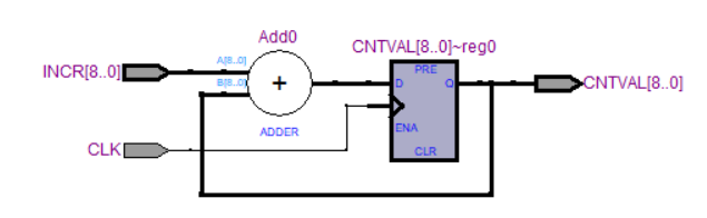
Counter with count increment input /
module cnt_incr(
CLK , // clock
INCR , // counter increase value
CNTVAL); // counter value
input CLK;
input [9-1:0] INCR;
output [9-1:0] CNTVAL;
reg [9-1:0] CNTVAL;
always @ (posedge CLK) begin
CNTVAL <= INCR + CNTVAL;
end
endmodule // module cnt_incr
RTL diagram of the above two modules: