preface
Verilog, Xilinx ISE 13.4, BASYS2, modulo 60 counter
1, Development environment
Verilog language
1. Data type
Constant: parameter IN_width = 4;Can be used to define variable width
 Variable: wire Type: use assign Assignment; Input / output signal default
      reg Type: in always Internal assignment; Indicates the trigger output signal
 Spacer: space, TAB
 Annotators: single line//, multiline / **/
Logical value: 0, 1, X,Z
 key word: module, endmodule, input, output, wire, reg, and
assign Statements: data flow mode
always Statements: behavior
 Component instantiation: Structured
2. Program statement
(1) Process block:
Procedure statement(@(sensitive table)
begin(: Block name)
......
end
(2) case statement:
case(variable)
   Value 1: block 1
   Value 2: block 2
   ......
   default: Block 3
endcase
(3) if statement:
if(Condition 1)
    Block 1
else if(Condition 2)
    Block 2
else
    Block 3
(4) for statement
for(Expression 1;Expression 2;Expression 3)
	Block statement
Xilinx ISE 13.4
1. Composition and function:
Project management tool Project Navigator
Comprehensive tool (circuit schematic diagram, technical schematic diagram) XST
Simulation tool Isim
Constraint editing tools (text editor, graphical user interface editor, timing Constraint Editor) PlanAhead and Constraint Editor
Implement tool
Download the programming tool Impact
Online logic analyzer Chipscope
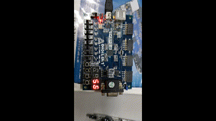
BASYS2 experimental board
1. Available resources
Four seven segment nixie tubes, eight LED indicators, four key switches, eight sliding switches, one PS/2 interface, one 8-bit VGA display interface, four 6-pin PMOD user expansion interfaces, configurable crystal oscillator and USB 2.0 interface.
2. Pin definition:
2, Design ideas
Create a 34 bit binary counter, intercept 25 to 28 bits as a bit number, 29 to 32 bits as a ten bit number, enter 1 when the number of bits is up to 10, and clear when the number of tens is up to 6. Display the number on the nixie tube through scanning, counting and decoding, so as to realize the function of analog-to-digital counter.
Determination of counting interval and scanning frequency:
Calculation formula: t is the time of change once, and n is the lowest digit intercepted
Take the counting interval of 1s, and the required digit i is about 26
If i=25, the counting interval is about 0.67s
Taking the scanning frequency of 100Hz, the required number of bits j is about 19
3, Verilog source file
module mo60(
    input clock,
    input reset,
    output [3:0] loc,//Nixie tube position
    output [7:0] num//Nixie tube pin
    );

	parameter i = 25;//Control the counting rate and take 0 during simulation; Take 25 when downloading (count every 0.7s)
	parameter j = 19;//Control the scanning rate and take 0 during simulation; Take 19 when downloading (scanning frequency 100Hz)
	reg [33:0] counter = 0;//count
	reg [33:0] counter0 = 0;//Count during reset, used to control the scanning rate
	reg [3:0] scan;//position
	reg [4:0] temp;//number
	reg [7:0] pin;//Pin
	reg [3:0] q1 = 0;//Ten
	reg [3:0] q0 = 0;//Bit

	//Counter
	always @(posedge clock)//Rising edge trigger
	begin
		//count
		if (reset)//High level active
			begin
				counter <= 0;
				counter0 <= counter0+1;
			end
		else
			begin
				counter0 <= 0;
				counter <= counter+1;
			end
		//carry
		if (counter[3+i:0+i] >= 10)
			begin
				counter[7+i:4+i] <= counter[7+i:4+i]+1;
				counter[3+i:0+i] <= 0;
			end
		if (counter[7+i:0+i] >= 8'b01100000)//60
			counter[7+i:0+i] <= 0;
		q1 = counter[7+i:4+i];
		q0 = counter[3+i:0+i];
	end

	//Scan @ access
	always @(counter[j] or counter0[j])
	begin
		if (reset)
			begin
				temp <= 0;
				if (counter0[j])
					scan <= 4'b1101;
				else
					scan <= 4'b1110;
			end
		else
			if (counter[j])
				begin
					scan <= 4'b1101;
					temp <= q1;
				end
			else
				begin
					scan <= 4'b1110;
					temp <= q0;
				end
	end

	//display
	always @(temp)
	begin
			case(temp)
				0: pin = 8'b00000011;//The last digit represents the decimal point
				1: pin = 8'b10011111;
				2: pin = 8'b00100101;
				3: pin = 8'b00001101;
				4: pin = 8'b10011001;
				5: pin = 8'b01001001;
				6: pin = 8'b01000001;
				7: pin = 8'b00011111;
				8: pin = 8'b00000001;
				9: pin = 8'b00001001;
				default: pin = 8'b01100001;//Other status display E
			endcase
	end

	assign loc = scan;
	assign num = pin;

endmodule
4, Test file
module test1;
	//Inputs
	reg clock;
	reg reset;
	//Outputs
   wire [3:0] loc;
   wire [7:0] num;
	//Clock cycle 20ns
	parameter PERIOD = 20;
	//instantiation
	mo60 uut (
		.clock(clock),
		.reset(reset),
		.loc(loc),
		.num(num)
	);
	//clock signal
	always begin
		clock = 1'b0;
		#(PERIOD/2) clock = 1'b1;
		#(PERIOD/2);
	end
	//Initial state
	initial begin
		clock = 1'b0;
		reset = 1;
		//The reset signal lasts for 500ns
		#500;
      	reset = 0;
	end
endmodule
5, Waveform simulation
1. Overall waveform when i=0 (counting interval is 1 cp) and j=0 (scanning interval is 1 cp)
Clock: clock, reset: reset, q1: the number displayed on the ten bits of the counter, q2: the number displayed on the four bits of the counter, loc: the level on the four nixie tubes, num: the level on the eight pins of the nixie tubes.
2. When the interval of cp (J) is 1, the interval of cp = 0
Take the waveform at the time of the yellow line as an example to explain the meaning of each variable. q1=5, q0=8, indicating that the number displayed on the nixie tube is 58, loc=1101, indicating that the nixie tube on the tenth digit is lit, num=01001001, indicating that all segments except the decimal point are lit, that is, the number 5 is displayed.
Due to the non blocking assignment, a state with a length of 1 pulse cycle error is generated at the carry (shown by the red arrow).
3. Local waveform when i=5 (counting interval is 0.6us) and j=3 (scanning frequency is 6MHz)
When i increases to 5, the duration of normal state is much longer than one pulse cycle, and the influence of error state can be ignored.
It can be inferred that when i=25 (counting interval is 0.7s) and j=19 (scanning frequency is 100Hz), the error state generated during carry can be ignored and does not affect the function of the counter.
6, Create timing and pin constraints
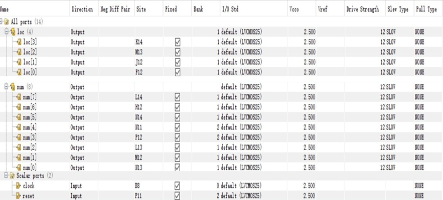
#Created by Constraints Editor (xc3s100e-cp132-4) - 2021/11/17
NET "clock" TNM_NET = "clock";
TIMESPEC TS_clock = PERIOD "clock" 20 ns HIGH 50 %;
# PlanAhead Generated physical constraints
NET "clock" LOC = B8;
NET "reset" LOC = P11;
NET "loc[3]" LOC = K14;
NET "loc[2]" LOC = M13;
NET "loc[1]" LOC = J12;
NET "loc[0]" LOC = F12;
NET "num[7]" LOC = L14;
NET "num[6]" LOC = H12;
NET "num[5]" LOC = N14;
NET "num[4]" LOC = N11;
NET "num[3]" LOC = P12;
NET "num[2]" LOC = L13;
NET "num[1]" LOC = M12;
NET "num[0]" LOC = N13;
7, Generate bit file, download to the development board
summary
Never learned Verilog
Despair~