Book "the art of hardware architecture: design methods and technologies of digital circuits"
(1) Metastable state
1.1 concept
-
Caused by violation of the set-up time and hold time of the trigger
-
In the window of the rising edge of the clock, the data changes and the output is unknown or metastable
- Metastable window
Metastable window -The larger the window, the higher the probability of entering metastable state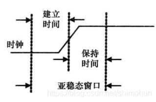
1.2 hazards
-
Output burr
-
It is temporarily unstable and takes a long time to return to stable state
-
Generally, it takes 1 ~ 2 time cycles to return to the steady state
1.3 MTBF
-
Meaning: reciprocal of failure rate
M T B F = e ( t τ / τ ) W f c f d (1.1) MTBF =\frac {e(t_\tau/\tau)} {W f_c~f_d} \\\tag{1.1} MTBF=Wfc fde(tτ/τ)(1.1) -
explain
- t τ t_\tau t τ : the resolution time allowed to exceed the normal transmission delay time of the device
- τ \tau τ : time constant of metastable state (analytical) of trigger
- W W W: Metastable window
- f c f_c fc: clock frequency
- f d f_d fd: asynchronous signal edge frequency
-
Details: omitted
1.4 occurrence scenario
-
As long as the establishment time and holding time are violated, metastability will occur:
- The input signal is asynchronous
- Clock offset / swing (rise / fall time) above tolerance
- The signal operates at two different frequencies or at the same frequency but with different phase and offset
- The combined delay changes the data input of the trigger in the metastable window
-
Metastable state can not be eradicated, but can only reduce the probability of its occurrence
1.5 methods to avoid metastable state
1.5. 1. The clock cycle is long enough
- If the performance is not evaluated, you can ensure that the clock cycle is long enough
- **Clock cycle > quasi steady state resolution time**
- The method is simple, but not practical
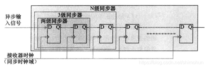
1.5. 2 use multi-stage synchronizer
- The first complete clock cycle solves the metastable problem
-
be careful:
An asynchronous signal should not be synchronized by two or more synchronizers, which will lead to the risk that the output of multi-level synchronizer will produce different signals
-
Code: take two-stage synchronizer as an example (common)
Commonly known as "two beats"
//Two stage synchronizer
module	demo(
	input	wire	sys_clk,
    input	wire	sys_rst_n,

    input	wire	date_in,
    output	reg		date_out
),

	reg		date_in_reg0;
	reg		date_in_reg1;

    always @(posedge sys_clk or negedge sys_rst_n) begin
        if(!sys_rst_n)
            date_in_reg0 <= 1'b0;
        else
           	date_in_reg0 <= date_in;
    end

    always @(posedge sys_clk or negedge sys_rst_n) begin
        if(!sys_rst_n)
            date_in_reg1 <= 1'b0;
        else
           	date_in_reg1 <= date_in_reg0;
    end

    assign	date_out = date_in_reg1 ;

endmodule
-
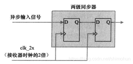
Optimization scheme: multi-stage synchronizer with clock frequency doubling
-
Limitation of the scheme: the limitation of using the above "two beats" is obvious. It takes a long time to respond to asynchronous input signals
-
Solution: double the frequency of the input clock as the clock input of two synchronous flip flops
Frequency doubling of clock with PLL
Multistage synchronizer with clock frequency doubling circuit
-
The code is as follows:
//Two stage synchronizer
module	demo(
	input	wire	sys_clk,
    input	wire	sys_rst_n,

    input	wire	date_in,
    output	reg		date_out
),

	reg		date_in_reg0;
	reg		date_in_reg1;

    always @(posedge sys_clk_2x or negedge sys_rst_n) begin
        if(!sys_rst_n)
            date_in_reg0 <= 1'b0;
        else
           	date_in_reg0 <= date_in;
    end

    always @(posedge sys_clk_2x or negedge sys_rst_n) begin
        if(!sys_rst_n)
            date_in_reg1 <= 1'b0;
        else
           	date_in_reg1 <= date_in_reg0;
    end

    assign	date_out = date_in_reg1;

    pll pll_inst(
        .clk_in		(sys_clk	),
        .c0			(sys_clk_2x	)
    );

endmodule
-
1.5. 3 type of synchronizer
1. High frequency → \rightarrow → low frequency
Method I:
-
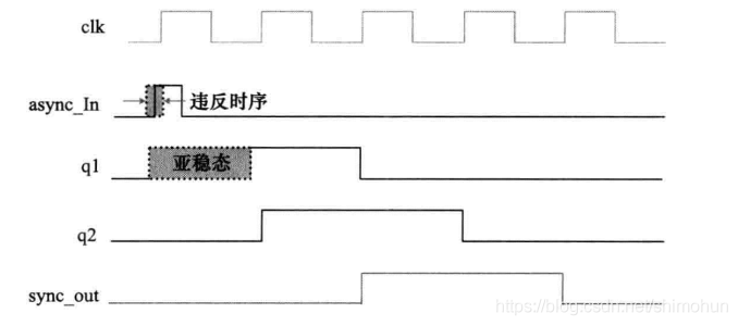
Circuit diagram
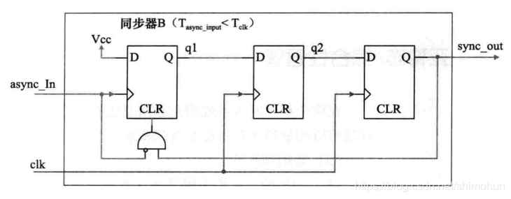
Description: inputs D and D of the first stage trigger V c c V_{cc} Vcc} is connected, and the clock signal is an asynchronous input signal. The other two flip flops are controlled by the system time (clk). A total of short pulses make q1 become a high level, which is output from sync_out after two clock (clk) edges
-
Sequence diagram
-
code
module demo (
    input	wire	    sys_clk,
    input	wire	    sys_rst_n,

    input	wire        clk_h,              //High speed clock, not used in this demo
    input	wire	    clk_l,              //Low speed clock, i.e. clk in the figure

    input	wire	    async_in,

    output	reg	        sync_out

);

//------------------------wire & reg-------------------//
//reg1 reset signal high level reset low level normal operation
wire	reg1_clr;

reg	    q1;
reg	    q2;


//-------------------------mian------------------------//
//reg_clr signal
assign reg1_clr = (!async_in) && sync_out;

//reg1
always @(posedge async_in or posedge reg1_clr) begin
    if(reg1_clr == 1'b1)
        q1 <= 1'b0;
    else
        q1 <= 1'b1;  //VCC in the figure
end

//reg2
always @(posedge clk_l) begin
    q2 <= q1;
end

//sync_out output
always @(posedge clk_l) begin
    sync_out <= q2;
end

endmodule
Method 2:
-
Thought:
Because it is high frequency → \rightarrow → low frequency, there may be signals in the high-frequency clock domain, and the clock in the low-frequency clock domain cannot be collected
Therefore, it is necessary to broaden the signal model in the high-frequency clock domain, so that the signal acquisition in the low-frequency clock domain can be obtained
Note: signal_b feedback to the high frequency clock domain is also cross clock domain, which also needs to be processed
-
method:
Pulse signal plus_ A at clk_h is widened to become level signal_a. Re clk_l pass, when confirming clk_l clear the signal after the "see" signal has been synchronized_ a. The implementation method is still * * "collect - take two shots - synchronize" *
-
code
module demo(
   input	wire	clk_h,
   input	wire	clk_l,
   input	wire	sys_rst_n,
   input	wire	pulse_a_in,

   output	wire    pulse_b_out,
   output	wire	b_out
);

//---------------- wire & reg ---------------------//

	reg					signal_a;
	reg					signal_b;
	reg					signal_b_r1;
	reg					signal_b_r2;
	reg					signal_b_a1;
	reg					signal_b_a2;

//---------------- mian --------------------------//
   //CLK in clock domain_ H, generate the widening signal_a
    always @(posedge clk_h or negedge sys_rst_n) begin
        if(!sys_rst_n)
            signal_a <= 1'b0;
        else if(pulse_a_in == 1'b1)  //Input signal pulse detected_ a_ If in is pulled high, signal is pulled high_ a
            signal_a <= 1'b1;
        else if(signal_b_a2 == 1'b1) //Signal detected_ b1_ If A2 is pulled high, signal is pulled low_ a
            signal_a <= 1'b0;
       	else
            signal_a <= signal_a;
    end

	//CLK in clock domain_ L, collect signal_a. Generate signal_b
    always @ (posedge clk_l or negedge sys_rst_n)begin
        if (!sys_rst_n)
			signal_b <= 1'b0;
		else
			signal_b <= signal_a;
	end

    //Multi level trigger processing (two levels here)
    always @ (posedge clk_l or negedge sys_rst_n)begin
        if (!sys_rst_n) begin
			signal_b_r1 <= 1'b0;
			signal_b_r2 <= 1'b0;
		end
		else begin
			signal_b_r1 <= signal_b;		//Yes, signal_b take two shots
			signal_b_r2 <= signal_b_r1;
		end
	end

	//CLK in clock domain_ Under a, collect signal_b_r1, used for feedback to pull down the spread signal_a
     always @ (posedge clk_h or negedge sys_rst_n) begin
        if (!sys_rst_n) begin
			signal_b_a1 <= 1'b0;
			signal_b_a2 <= 1'b0;
		end
		else begin
			signal_b_a1 <= signal_b_r1;	//Yes, signal_b_r1 takes two beats because it also involves cross clock domain
			signal_b_a2 <= signal_b_a1;
		end
	end

	assign	pulse_b_out =	signal_b_r1 & (~signal_b_r2);
	assign	b_out		=	signal_b_r1;

endmodule
2. Low frequency → \rightarrow → high frequency
-
There is no problem that the signal cannot be collected from low-frequency signal to high-frequency signal. Therefore, the method of two beats can be directly used for detection
-
code
// The code directly adopts the code of multi-level synchronizer
-
A special case - the output signal in the low frequency domain is generated by combinatorial logic
-
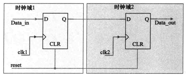
Circuit diagram
explain:
- Clock domain 1 is a low-frequency clock domain, and clock domain 2 is a high-frequency clock domain
- Data_in is generated by combinatorial logic, i.e. assign
- The shaded part of clock field 2 represents a multi-level synchronizer
-
code
module demo( input wire clk_l, input wire clk_h, input wire sys_rst_n, input wire date_in, output reg date_out ); reg date_l; reg date_h_0; reg date_h_1; //The signal of combinational logic first passes through the clock synchronization of low clock domain always @(posedge clk_l or negedge sys_rst_n) begin if(!sys_rst_n) date_l <= 1'b0; else date_l <= date_in; end //Date in high clock domain_ In synchronization always @(posedge clk_h or negedge sys_rst_n) begin if(!sys_rst_n) begin date_h_0 <= 1'b0; date_h_1 <= 1'b0; end else begin date_h_0 <= date_l; date_h_1 <= date_h_0; end end assign date_out <= date_h_1; endmodule -
1.6 Summary - reducing metastability
It is clear that metastability is unavoidable and can only reduce the probability of metastability
The following are several methods to reduce the probability of metastable state
- Using synchronizer
- Trigger with faster response (shorten metastable window) T w T_w Tw)
- Metastable hardening flip-flop is adopted (specially designed for high bandwidth and reducing the sampling time optimized for clock domain input circuit)
- Cascade trigger is used as synchronizer
- The probability of metastable failure of a common trigger is P P P. Then N N The probability of metastable failure of N flip flops is P N P^N PN
- Reduce sampling rate
- Avoid using d V / d t dV/dt Input signal when dV/dt is low