Basic circuit
1-bit full adder
module full_adder(
	input a,
	input b,
	input cin,

	output sum,
	output cout
	);
	assign {cout,sum}=a+b+cin;
endmoudle
| a | b | cin | sum | cout |
|---|---|---|---|---|
| 0 | 0 | 0 | 0 | 0 |
| 0 | 0 | 1 | 1 | 0 |
| 0 | 1 | 0 | 1 | 0 |
| 0 | 1 | 1 | 0 | 1 |
| 1 | 0 | 0 | 1 | 0 |
| 1 | 0 | 1 | 0 | 1 |
| 1 | 1 | 0 | 0 | 1 |
| 1 | 1 | 1 | 1 | 1 |
module full_adder(
	input a,
	input b,
	input cin,

	output sum,
	output cout
	);
	assign sum=a^b^cin;
	assign cout=(a&b)
				|(cin&b)
				|(cin&b);
endmoudle
4-bit full adder
module four_full_adder(
	input [3:0] a;
	input [3:0] b,
	input cin,

	output [3:0] sum,
	output cout
	);
	assign {cout,sum}=a+b+cin;
endmoudle
4-1 multiplexer
module four_mux(
	input [3:0] a,
	input [3:0] b,
	input [3:0] c,
	input [3:0] d,
	input [1:0] sel,

	output [3:0] mux_out
	);
	always@(*)
	begin
		case(sel)
			2'b00:mux_out=a;
			2'b01:mux_out=b;
			2'b10:mux_out=c;
			2'b11:mux_out=d;
		endcase
	end
endmodule
Frequency divider
Odd frequency divider
Odd frequency division by clock phase or
module any_odd_div(
	input clk,
	input rst_n,

	output div_clk
	);

	parameter odd = 5;
	reg [3:0] cnt1 , cnt2;
	reg clk_tem_pos , clk_tem_neg;

	always @ (posedge clk or negedge rst_n)
	begin
	if (!rst_n) begin
		cnt1 <= 4'b00;
		clk_tem_pos <= 1'b0;
		end
	else begin
		cnt1 <= (cnt1  == odd-1)?4'b0:cnt1+1'b1;
		clk_tem_pos <= (cnt1< (odd-1)/2)?1'b1:1'b0;
		end
	end

	always @ (negedge clk or negedge rst_n)
	begin
	if (!rst_n) begin
		cnt2 <= 4'b00;
		clk_tem_neg <= 1'b0;
		end
	else begin
		cnt2 <= (cnt2  == odd-1)?4'b0:cnt2+1'b1;
		clk_tem_neg <= (cnt2< (odd-1)/2)?1'b1:1'b0;
		end
	end

	assign div_clk = clk_tem_pos|clk_tem_neg;
endmodule
Simulation:
`timescale 1ns / 1ps
module any_odd_div_tb( );
    reg clk;
    reg rst;
    //reg clk_out;//concurrent assignment to a non-net 'clk_out' is not permitted
    wire clk_out;

    initial
    begin
        clk=0;
        rst=0;
        #50;
        rst=1;
    end

    always
    begin
    #5
    clk=~clk;
    end

    any_odd_div u1(.clk(clk),.rst_n(rst),.div_clk(clk_out));

endmodule
Even frequency divider
edge detection
Detect the edge of the input signal. When it is detected that the signal is from low to high, the corresponding signal output is high.
module edge_detection(
	input x,
	input clk,
	output y_pos,y_neg);

	reg x_fron;
	always@(posedge clk)
		begin
		x_fron<=x;
		end

	assign y_pos=~x_fron&x;//posedge
	assign y_neg=x_fron&~x;//nededge
endmodule
simulation
    module edge_dec_tb();

    reg clk;
    reg x_in;

    wire y_pos,y_neg;

    initial
    begin
    clk=0;
    x_in=0;
    #40
    x_in=1;
    #40
    x_in=0;
    end

    always #5 clk=~clk;

    edge_detection u2(.x(x_in),.clk(clk),.y_pos(y_pos),.y_neg(y_neg));


endmodule
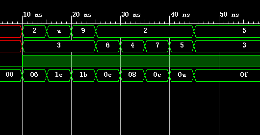
Sequence detection
The title comes from the Internet
Sequence detection: it is required to detect "10010" in the input code stream, and if it is detected, data_out output 1,. At the same time, overlap detection needs to be excluded, for example:
Input: 1-0-0-1-0_0-1-0-0-1-0-XXXXX
Output: 0-0-0-0-1_0-0-1-0-0-1-XXXXX
The second 1 in the output stream is the overlapping output, which needs to be excluded.
Two stage state machine:
There are two always block s that separate sequential logic from combinatorial logic. The current state and the next state are switched in the sequential logic, and the combinational logic realizes each input, output and state judgment.
Three stage state machine:
coding style:cur_state and next_state;
There are three always block s. One timing logic uses synchronous timing to describe the state transition, one uses combinatorial logic to judge the state transition conditions and describe the state transition law, and the third module uses synchronous timing to describe the output of each state. The output of sequential logic solves the burr problem of two-stage combinational logic.
A brief summary is:
**Moore state machine: * * the last state is the completed state.
**Mealy state machine: * * there is one less state than Moore state machine, and the last state judges the output at the same time.
Three stage state machine:
Write cur in the first section of temporal logic_ State and next_ Transfer relationship between states
In the second paragraph, write case, the conditions for each state to change to the next state
Third segment write output
Two stage state machine:
The first paragraph is the same as above
The second segment writes state transfer and output at the same time.
Two stage state machine
Different from the three-stage formula, out needs to be reg type
`timescale 1ns / 1ps


module seq_dec(
	input seq_in,
	input clk,
	input rst_n,
	//procedural assignment to a non-register test_out is not permitted
	output reg test_out);

//Define six states
	parameter 	IDLE        = 6'b000001,
				fir_1       = 6'b000010,
				sec_10      = 6'b000100,
				thir_100    = 6'b001000,
				fou_1001    = 6'b010000,
				out_10010   = 6'b100000;


	reg [5:0] cur_state;
	reg [5:0] next_state;

	always@(posedge clk or negedge rst_n)
		if (!rst_n) begin
			//test_ out <= 1'b0; Duplicate definition
			cur_state  <= IDLE;
			//next_ state <= IDLE;// Multiple definitions
			end
		else begin
			cur_state <= next_state;
			end

	always@(*)
		begin
		case(cur_state)
            IDLE        :begin
                next_state = (seq_in)? fir_1    : IDLE;
                test_out=1'b0;
            end
            fir_1       :begin
                next_state = (seq_in)? fir_1    : sec_10;
                test_out=1'b0;
            end
            sec_10      :begin
                next_state = (seq_in)? fir_1    : thir_100;
                test_out=1'b0;
            end
            thir_100    :begin
                next_state = (seq_in)? fou_1001 : IDLE;
                test_out=1'b0;
            end
            fou_1001    :begin
                next_state = (seq_in)? fir_1    : out_10010;
                test_out=1'b0;
            end
            out_10010   :begin
                next_state = (seq_in)? fir_1    : IDLE ;
                test_out=1'b1;
            end
            default     :begin
                next_state = IDLE ;
                test_out=1'b0;
            end
        endcase
        end


endmodule
Three stage state machine
module seq_dec(
	input seq_in,
	input clk,
	input rst_n,
	output test_out);

//Define six states
	parameter 	IDLE        = 6'b000001,
				fir_1       = 6'b000010,
				sec_10      = 6'b000100,
				thir_100    = 6'b001000,
				fou_1001    = 6'b010000,
				out_10010   = 6'b100000;


	reg [5:0] cur_state;
	reg [5:0] next_state;

	always@(posedge clk or negedge rst_n)
		if (!rst_n) begin
			//test_ out <= 1'b0; Duplicate definition
			cur_state  <= IDLE;
			//next_ state <= IDLE;// Multiple definitions
			end
		else begin
			cur_state <= next_state;
			end

	always@(*)
		begin
		case(cur_state)
            IDLE        :next_state = (seq_in)? fir_1    : IDLE;
            fir_1       :next_state = (seq_in)? fir_1    : sec_10;
            sec_10      :next_state = (seq_in)? fir_1    : thir_100;
            thir_100    :next_state = (seq_in)? fou_1001 : IDLE;
            fou_1001    :next_state = (seq_in)? fir_1    : out_10010;
            out_10010   :next_state = (seq_in)? fir_1    : IDLE ;
            default     :next_state = IDLE ;
        endcase
        end

    assign test_out=(cur_state == out_10010)?1'b1:1'b0;

endmodule
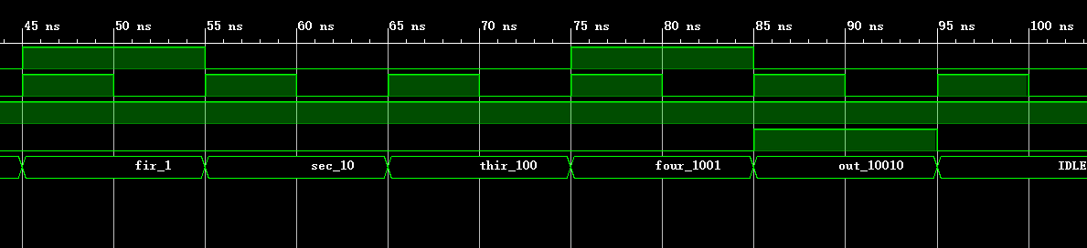
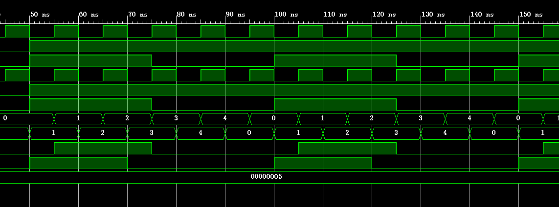
Testbench
`timescale 1ns / 1ps

module seq_dec_tb( );

    reg seq_in;
    reg clk;
    reg rst_n;

    wire test_out;

    initial
    begin
    clk=0;
    seq_in=0;
    rst_n=0;
    #5
    seq_in=1;
    rst_n=1;//Don't forget to pull up the reset signal
    #10
    seq_in=0;
    #10
    seq_in=0;
    #10
    seq_in=0;
    #10
    seq_in=1;
    #10
    seq_in=0;
    #10
    seq_in=0;
     #10
    seq_in=1;
    #10
    seq_in=0;
    #10
    seq_in=0;
     #10
    seq_in=1;
    end

    always #5 clk=~clk;

    seq_dec u1(.seq_in(seq_in),.clk(clk),.rst_n(rst_n),.test_out(test_out));

    reg [127:0] next_state_name;

   always@(*) begin
        case(u1.cur_state)//Directly use the name of the module instantiation
	        6'b000001:   next_state_name= "IDLE"   ;
			6'b000010:   next_state_name= "fir_1";
			6'b000100:   next_state_name= "sec_10";
			6'b001000:   next_state_name= "thir_100";
			6'b010000:   next_state_name= "four_1001";
			6'b100000:   next_state_name= "out_10010";
			default  :   next_state_name= "IDLE"  ;
			endcase
		end
endmodule
Shift register method
`timescale 1ns / 1ps

//Use the register to save the value of each entry sequence. When the total length is 10010, the output is 1
//At the same time, clear the value of reg when the sequence is 10010 to avoid overlapping output

module seq_dec(
	input seq_in,
	input clk,
	input rst_n,
	output test_out);

    reg [4:0] ud_test;

    always@(posedge clk or negedge rst_n)
        begin
        if(!rst_n)
            ud_test<=5'b0;
        else
            ud_test<=(ud_test==5'b10010)?{4'b0,seq_in}:{ud_test[3:0],seq_in};
        end

    assign test_out=(ud_test==5'b10010)?1'b1:1'b0;

endmodule
four × 4 look up table multiplier
The core of look-up table method is to store all possible results of multiplication, and then combine the two multiplied data as an address to directly find the corresponding results.
Implementation of 4-bit Multiplier: call 2-bit multiplier, that is, decompose the high-order wide data into low-order wide data, and then call the look-up table multiplier.
For 2N bit data a, it can be decomposed into A=A1 × 2 ^ n + A0, A1 is the high N bit and A0 is the low N bit
For 2-bit multipliers, A = 2 × A1 + A0,B = 2 × B1 + B0;
Multiplication expansion: a × B = 4 × A1 × B1 + 2 × A1 × B0 + 2 × A0 × B1 + A0 × B0;
For 4-bit multipliers, A = 4 × A1+ A0 ,B = 4 × B1 + B0;
Multiplication expansion: a × B = 16 × A1 × B1 + 4 × A1 × B0 + 4 × A0 × B1 + A0 × B0;
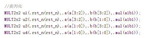
`timescale 1ns / 1ns


module inst(
    input rst_n,
    input [3:0] a,
    input [3:0] b,
    output  wire [7:0] mul4
    );
    //A×B = 16×A1×B1 + 4×A1×B0 + 4×A0×B1 + A0×B0
    //reg [3:0] a1b1;concurrent assignment to a non-net
    wire [3:0] a1b1;
    wire [3:0] a1b0;
    wire [3:0] a0b1;
    wire [3:0] a0b0;

    //Materialization
    MULT2x2 u1(.rst_n(rst_n),.a(a[3:2]),.b(b[3:2]),.mul(a1b1));
    MULT2x2 u2(.rst_n(rst_n),.a(a[3:2]),.b(b[1:0]),.mul(a1b0));
    MULT2x2 u3(.rst_n(rst_n),.a(a[1:0]),.b(b[3:2]),.mul(a0b1));
    MULT2x2 u4(.rst_n(rst_n),.a(a[1:0]),.b(b[1:0]),.mul(a0b0));

    //assign mul4 = (!rst_n)? 8'b0:{a1b1,4'b0}+{a1b0,3'b0}+{a0b1,3'b0}+a0b0;
    assign mul4 = (!rst_n)? 8'b0:{a1b1,4'b0}+{a1b0,2'b0}+{a0b1,2'b0}+a0b0;

endmodule

module MULT2x2(
    input rst_n,
    input [1:0] a,//A = 2×A1 + A0
    input [1:0] b,//B = 2×B1 + B0
    output reg[3:0] mul
    );

    always @(*) begin
        if (!rst_n)
            mul=4'd0;
        else begin
        case({a,b})//Don't follow begin after case
                4'b0000:mul=4'd0;
                4'b0001:mul=4'd0;
                4'b0010:mul=4'd0;
                4'b0011:mul=4'd0;
                4'b0100:mul=4'd0;
                4'b0101:mul=4'd1;
                4'b0110:mul=4'd2;
                4'b0111:mul=4'd3;
                4'b1000:mul=4'd0;
                4'b1001:mul=4'd2;
                4'b1010:mul=4'd4;
                4'b1011:mul=4'd6;
                4'b1100:mul=4'd0;
                4'b1101:mul=4'd3;
                4'b1110:mul=4'd6;
                4'b1111:mul=4'd9;
        endcase
        end
    end

endmodule
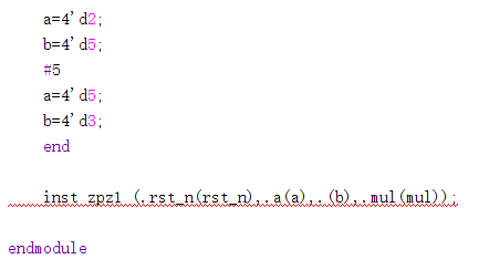
testbench
`timescale 1ns / 1ns

module inst_tb();

    reg [3:0]a;
    reg [3:0]b;
    reg rst_n;
    wire [7:0] mul;

    initial
    begin
    #5
    rst_n=0;
    #5
    rst_n=1;
    a=4'd2;
    b=4'd3;
    #5
    a=4'd10;
    b=4'd3;
    #5
    a=4'd9;
    b=4'd3;
    #5
    a=4'd2;
    b=4'd6;
    #5
    a=4'd2;
    b=4'd4;
    #5
    a=4'd2;
    b=4'd7;
    #5
    a=4'd2;
    b=4'd5;
    #5
    a=4'd5;
    b=4'd3;
    end

    inst zpz1 (.rst_n(rst_n),.a(a),.b(b),.mul4(mul));

endmodule
64bits is detected as the lowest bit of 1
module low_bit_dec(
    input [63:0] data,
    output reg [5:0] out_nm
);
    integer i;
    always @(*)
        begin
        for (i=0; i < 63 ; i=i+1)
            if (data[i] == 1'b1)
                out_nm = i;
            else
               //wrong: out_nm= 6'bx;
                out_nm= out_nm;
    end

endmodule
Multiply two 8-digit numbers
Using a cycle, each of a number and its corresponding number are added with the subsequent phase shift.
`timescale 1ns / 1ns
//
// Company:
// Engineer:
//
// Create Date: 2022/02/24 18:47:02
// Design Name:
// Module Name: inst
// Project Name:
// Target Devices:
// Tool Versions:
// Description:
//
// Dependencies:
//
// Revision:
// Revision 0.01 - File Created
// Additional Comments:
//
//


module inst(
    input [7:0] data1,
    input [7:0] data2,
    input       rst_n,
    output [15:0] mul_ans
);

    reg [15:0] mid_ans;
    reg [15:0]
    reg [7:0] low_ans;


    integer i;
    always @(*) begin
        if(!rst_n) begin
            mid_ans=16'b0;
            low_ans=8'b0;
            end
        else begin
            for (i=1; i < 8 ; i=i+1)
                mid_ans=(data1[i])? (mid_ans + (data2 << i)):mid_ans;
             low_ans={8{data1[0]}}&data2;
        end
    end

    assign mul_ans=mid_ans+low_ans;

endmodule
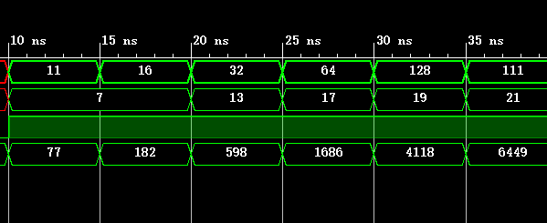
The result is incorrect. Error reason: the value of each time is not cleared, including the previous value, i.e. 182 + 32 * 13 = 598
Change:
`timescale 1ns / 1ns

module  8x8mul(
    input [7:0] data1,
    input [7:0] data2,
    input       rst_n,
    output [15:0] mul_ans
);

    reg [15:0] mid_ans;
    wire [15:0] ap_data2;
    reg [7:0] low_ans;

    assign ap_data2=data2;

    integer i;
    always @(*) begin
        mid_ans=16'b0;//There is no error in multiple assignments in the same block
        if(!rst_n) begin
			 mid_ans=16'b0;
            low_ans=8'b0;
            end
        else begin
            for (i=1; i < 8 ; i=i+1)
                mid_ans=(data1[i])? (mid_ans + (ap_data2 << i)):mid_ans;
            low_ans={8{data1[0]}}&data2;
        end
    end

    assign mul_ans=mid_ans+low_ans;

endmodule
Decimal counter
module 10counter(
    input clk,
    input rst_n,
    output reg [3:0] ctr
);

    always @(posedge clk) begin
        if (!rst_n)
            ctr=4'b0;
        else
            ctr=((ctr+1'b1)==4'b1010)?4'b0:ctr+1'b1;
    end
endmodule
DFF description
module DFF(
    input clk,
    input rst_n,
    input d,

    output reg q
);
    always @(posedge clk) begin
        if (!rst_n)
            q<=1'b0;
        else
            q<=d;
    end

endmodule
Comparison circuit - retain maximum
module comparator(
    input clk,
    input rst_n,
    input [7:0] a,
    input [7:0] b,

    output reg [1:0] q
);
    always @(*) begin
        if (a > b)
            q <= 2'b01;
        else if (a == b)
            q <= 2'b00;
         else
            q <= 2'b10;
    end

endmodule
Single hot code detection
Given A 4-bit signal A, design logic to judge whether A is A single hot code and set the output as Y. if A is A single hot code, Y outputs 1; if not, 0
The idea is to sum the digits
module one_hot(
    input clk,
    input rst_n,
    input [3:0] a,

    output reg  q
);
    always @(*) beginone_hot
        if ((a[0]+a[1]+a[2]+a[3]) == 1)
            q <= 1'b1;//one hot bit
         else
            q <= 1'b0;
    end

endmodule
Settable hex cycle counter
module load_cnt(


    input clk,
    input rst_n,
    input load,
    output reg [2:0] out
);
    parameter load_N = 2;

    always @(posedge clk) begin
        if (!rst_n)
            out='b0;
        else if(load)
            out = load_N;
        else
            out = ((out+1'b1)==7)?'b0:out+'b1;
    end

endmodule
Parity bit
Parity bit is a binary number that represents a given location number. The number of 1 is an odd or even binary number. Parity bit is the simplest error detection code.
Bitwise XOR: even check
Bitwise XOR Negation: odd check
Deburring
Causes of burrs
When the signal passes through the wiring and logic gate inside the FPGA device, there is generally a certain delay. The size of the delay is related to the length of the connection and the number of gate units. At the same time, it is also affected by the manufacturing process, working voltage, temperature and other conditions of the device. In addition, the high / low level conversion of the signal also needs a certain transition time. Due to the influence of these factors, when the level value of multi-channel signal changes, at the moment of signal change, the output of combinational logic has sequence, rather than changing at the same time, which often leads to some incorrect "burrs".
There are two types of circuits for "burr" signals. The first is the asynchronous circuit with different delay after the input signal is wired inside the FPGA; The second is because the internal signal changes backward during programming. When multiple signals are correlated, if the first signal changes backward, the subsequent signals will produce uncertainty, resulting in "burr". The existence of "burr" indicates that the circuit is unstable, so it is likely to lead to the misoperation of the whole system.
terms of settlement:
Combinational logic circuit: add synchronous clock in the circuit, that is, input and output plus trigger to make the output signal change synchronously with the clock.
The discriminant assignment of the internal signal in the program does not change immediately, but there is a delay. This is also the most likely situation to produce "burr": the method of adding trigger is used to eliminate "burr"
Serial parallel conversion
module inst(


    input clk,
    input rst_n,
    input a,
    output reg [7:0] b
);

    always @(posedge clk) begin
        if (!rst_n)
            b='b0;
        else
            b = {b[6:0],a};
    end

endmodule
Key shaking elimination 15ms
When the mechanical key is pressed and bounced, it will shake for a short time, and the shaking time generally lasts for 15ms.
In the design with few keys, the keys are often reused. The common method is to judge according to the length and short of key pressing time. Therefore, key reuse often uses the falling edge after key debounce (if the key is pressed with high potential).
Assume key is key_in, set a sampling register sw_rst records the value of the last clock
Judgment key_ Whether in is consistent with the value of the previous register. If it is inconsistent, it indicates that the key action may occur (detection of rising and falling edges), and the key action is registered in edge_en,edge_n = 1 indicates the action of generating the key
Then start the 15ms counter to count. After 15ms delay, set the key_ Assign in value to out
module key (
    input clk,
    input rst_n,
    input key_in,
    output reg sw_out
);
    reg sw_rst;//The key itself is 1, and it is 0 after being pressed

    always @(posedge clk or negedge rst_n) begin
        if (!rst_n) begin
            sw_rst <= 1'b1;
        end
        else begin
            sw_rst <= key_in;
        end
    end

    wire pos_ed,neg_ed;
    assign pos_ed = !sw_rst & key_in;//Rising edge
    assign neg_ed = sw_rst & !key_in; //Falling edge

    wire edge_en;
    assign edge_en = pos_ed | neg_ed; //Check whether the key value changes (rising edge and falling edge)

    reg [19:0] cout ;
    always @ (posedge clk or negedge rst_n) begin
		if(!rst_n) begin
			count <= 0;
		end
		else if(edge_en) begin
			count <= 0;
		end
		else begin
			count <= count + 1;
		end

	end

    always @(posedge clk or negedge rst_n) begin
        if (!rst_n)
            sw_out <= 1'b1;
        else
            sw_out <= key_in;
    end


endmodule