catalogue
3.2.3.1 4-bit Shift Register(shift4)
3.2.3.2 Left/right rotator(rotate100)
3.2.3.3 Left/right arithmetic shift by 1 or 8(shift18)
3.2.3.5 3-bit LFSR(Mt2015 lfsr)
3.2.3.7 shift register(Exams/m2014 q4k)
3.2.3.8 shift register(Exams/m2014 q4b)
3.2.3.9 3-input LUT(Exams/ece241 2013 q12)
Foreword
HDLbits website is as follows
Problem sets - HDLBits (01xz.net)
Starting from this issue, we continue to study Chapter 3 Circuits of HDL bits. The content of this issue is 3.2 3 Shift Registers
3.2.3.1 4-bit Shift Register(shift4)
A four bit shift register (shift right) is constructed, which has the functions of asynchronous reset, synchronous set and enable.
- areset: resets the shift register to 0
- Load: load the shift register with data[3:0] instead of shifting
- ena: shift right (q[3] becomes 0, q[0] moves out and disappears)
- q: Contents of shift register
If load and ena are both valid (1), load has a higher priority
Solution:
module top_module(
    input clk,
    input areset,  // async active-high reset to zero
    input load,
    input ena,
    input [3:0] data,
    output reg [3:0] q);
    always@(posedge clk,posedge areset)
        begin
            if(areset)
                q<=4'd0;
            else if(load)
                q<=data;
            else if(ena)
                q<={1'b0,q[3:1]};
        end
endmodule
Distinguish priorities, and set > Load > ENA
3.2.3.2 Left/right rotator(rotate100)
Build a 100 bit left/right shift register with synchronous setting and left/right enabling functions. In this problem, the shift register will not be discarded or supplemented with 0, but cyclic shift.
- Load: load the shift register with data[99:0] instead of shifting
- ena[1:0]: select whether to cycle and the direction of the cycle (2 'b01 moves 1 bit right, 2' b10 moves 1 bit left, 2 'b00 and 2' b11 do not cycle)
- q: Contents of shift register
If load and ena are both valid (1), load has a higher priority
Solution:
module top_module(
    input clk,
    input load,
    input [1:0] ena,
    input [99:0] data,
    output reg [99:0] q);
    always@(posedge clk)
        begin
            if(load)
                q<=data;
            else
                begin
                    case(ena)
                        2'b01:q<={q[0],q[99:1]};
                        2'b10:q<={q[98:0],q[99]};
                        default:q<=q;
                    endcase
                end
        end
endmodule
3.2.3.3 Left/right arithmetic shift by 1 or 8(shift18)
Build a 64 bit arithmetic shift register with synchronous setting function. The shifter can move 1 bit or 8 bits left and right, which is selected by amount.
The sign bit of arithmetic right shift remains unchanged, that is, the signed number is divided by the power of 2, while the logical right shift needs to be filled with zero.
- Load: load the shift register with data[63:0] instead of shifting
- ena: select whether to shift
- amount: 2 'b00 shifts left by 1 bit, 2' b01 shifts left by 8 bits, 2 'b10 shifts right by 1 bit, and 2' b11 shifts right by 8 bits
- q: Contents of shift register
Hint: a 5-digit 11000 arithmetic right shift of 1 bit is 11100, while a logical right shift will generate 01100
Similarly, the arithmetic shift right of 01000 by 1 bit is 00100, and the logical shift right will produce the same result because the sign bit is non negative.
Solution:
module top_module(
    input clk,
    input load,
    input ena,
    input [1:0] amount,
    input [63:0] data,
    output reg [63:0] q);
    always@(posedge clk)
        begin
            if(load)
                q<=data;
            else if(ena)
                begin
                    case(amount)
                        2'b00:q<={q[62:0],1'b0};
                        2'b01:q<={q[55:0],8'b0};
                        2'b10:q<={q[63],q[63:1]};
                        2'b11:q<={{8{q[63]}},q[63-:56]};
                    endcase
                end
        end
endmodule
3.2.3.4 5-bit LFSR(Lfsr5)
Linear feedback shift registers usually have several XOR gates to generate the next state of the shift register. Galois LFSR is a special structure that XOR the "tap" bit with the output bit to produce its next value. If the tap bit is carefully selected, the LFSR can be made to the maximum length. The LFSR with the maximum length of N bits has 2^n-1 states before repetition (all 0 states cannot be reached).
The following figure shows a 5-bit maximum length Galois LFSR with its tap in bits 5 and 3. (tap is usually numbered from 1). Note that for consistency, I drew the XOR gate in bit 5, but one of the XOR gate inputs is 0.
reset resets the LFSR to 1
Hint: the first several States starting from 1 are 00001, 10100, 01010, 00101 LFSR should cycle through 31 states before returning to 00001.
Solution:
module top_module(
    input clk,
    input reset,    // Active-high synchronous reset to 5'h1
    output [4:0] q
);
    always@(posedge clk)
        begin
            if(reset)
                q<=5'h1;
            else
                q<={q[0]^1'b0,q[4],q[3]^q[0],q[2],q[1]};
        end

endmodule
3.2.3.5 3-bit LFSR(Mt2015 lfsr)
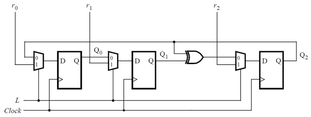
Write Verilog code for this sequential circuit (there can be sub modules, but the top level must be named top_module). Suppose you want to implement the circuit on the DE1-SoC board. Connect R input to SW switch, Clock to KEY[0], L to KEY[1]. Connect Q output to red LEDR
This circuit is an example of a linear feedback shift register (LFSR). The maximum period LFSR can be used to generate pseudo-random numbers because it loops 2^n-1 combinations before repetition. All zero combinations do not appear in this sequence.
Solution:
module top_module (
	input [2:0] SW,      // R
	input [1:0] KEY,     // L and clk
	output [2:0] LEDR);  // Q

    always@(posedge KEY[0])
        begin
            LEDR[2]<=KEY[1]?SW[2]:(LEDR[2]^LEDR[1]);
            LEDR[1]<=KEY[1]?SW[1]:LEDR[0];
            LEDR[0]<=KEY[1]?SW[0]:LEDR[2];
        end
endmodule
3.2.3.6 32-bit LFSR(Lfsr32)
Build a 32-bit Galois LFSR, in which 32, 22, 2 and 1 bits have tap
This question is long enough that you need to use vectors instead of 32 instantiations of DFF.
Solution:
module top_module(
    input clk,
    input reset,    // Active-high synchronous reset to 32'h1
    output [31:0] q
);
    reg[31:0]q_next;
    always@(*)
        begin
            q_next=q[31:1];
            q_next[31]=q[0]^1'b0;
            q_next[21]=q[0]^q[22];
            q_next[1]=q[0]^q[2];
            q_next[0]=q[0]^q[1];
        end
    always@(posedge clk)
        begin
            if(reset)
                q<=32'h1;
            else
                q<=q_next;
        end

endmodule
3.2.3.7 shift register(Exams/m2014 q4k)
The following circuits are implemented:
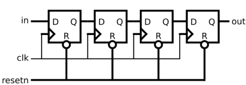
Solution:
module top_module (
	input clk,
	input resetn,
	input in,
	output out
);

	reg [3:0] sr;

	// Create a shift register named sr. It shifts in "in".
	always @(posedge clk) begin
		if (~resetn)		// Synchronous active-low reset
			sr <= 0;
		else
			sr <= {sr[2:0], in};
	end

	assign out = sr[3];		// Output the final bit (sr[3])

endmodule
3.2.3.8 shift register(Exams/m2014 q4b)
Consider the following n-bit shift register circuit:
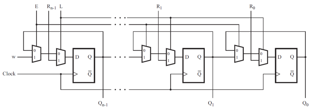
Write a top-level Verilog module (named top_module) for the shift register, assuming n = 4. Instantiate four copies of the MUXDFF sub circuit in the top-level module. Suppose you want to implement the circuit on the DE2 board.
- Connect the R input to the SW switch
- clk connect to KEY[0]
- E connect to KEY[1]
- L connect to KEY[2]
- w connect to KEY[3]
- Input connected to red LEDR[3:0]
(reuse from) Exams/2014 q4a - HDLBits MUXDFF.)
Solution:
module top_module (
    input [3:0] SW,
    input [3:0] KEY,
    output [3:0] LEDR
); //

    MUXDFF DFF3(KEY[0],KEY[3],SW[3],KEY[1],KEY[2],LEDR[3]);
    MUXDFF DFF2(KEY[0],LEDR[3],SW[2],KEY[1],KEY[2],LEDR[2]);
    MUXDFF DFF1(KEY[0],LEDR[2],SW[1],KEY[1],KEY[2],LEDR[1]);
    MUXDFF DFF0(KEY[0],LEDR[1],SW[0],KEY[1],KEY[2],LEDR[0]);

endmodule

module MUXDFF (
    input clk,
    input w, R, E, L,
    output Q
);
    wire temp1,temp2;
    assign temp1=(E?w:Q);
    assign temp2=(L?R:temp1);
    always@(posedge clk)
    begin
        Q<=temp2;
    end

endmodule
3.2.3.9 3-input LUT(Exams/ece241 2013 q12)
In this problem, you will design a circuit for 8x1 memory, where writing to memory is done by moving in bits, and reading is "random access", just like in typical RAM. You will then use this circuit to implement the 3-input logic function.
Firstly, an 8-bit shift register is constructed with 8 D flip flops. Tag from Q[0] Trigger output of Q [7]. The shift register input shall be called S, It provides the input of Q[0] (MSB moves in first). enable enables the input to control whether to shift. Then, expand the circuit to have three additional inputs A, B, C and one output Z. the behavior of the circuit should be as follows: when ABC is 000, Z=Q[0], when ABC is 001, Z=Q[1], and so on. Your circuit should contain only 8-bit shift registers and multiplexers. (in addition, the circuit is called A 3-input look-up table (LUT)).
Solution:
module top_module (
	input clk,
	input enable,
	input S,

	input A, B, C,
	output reg Z
);

	reg [7:0] q;

	// There are many ways to build an 8-out-of-1 data selector, such as case statements in combinational logic blocks
	assign Z = q[ {A, B, C} ];


	// When enabled, move 1 bit to the left, discard q[7], and move to S
	always @(posedge clk) begin
		if (enable)
			q <= {q[6:0], S};
	end


endmodule
Learned new expressions
assign Z = q[ {A, B, C} ];
LUT is very important and is used to replace gate circuit in FPGA