1, Introduction to AXI
1.AXI overview
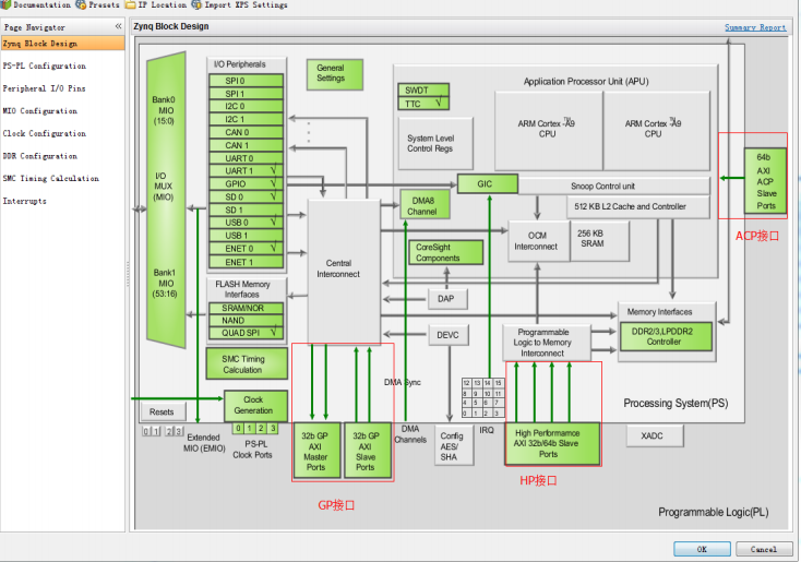
ZYNQ closely combines high-performance ARM Cotex-A series processors with high-performance FPGA in a single chip. After integrating processors with different process characteristics and FPGA on one chip, the interconnection path between on-chip processor and FPGA has become the top priority of ZYNQ chip design. If the data interaction between Cotex-A9 and FPGA becomes a bottleneck, the performance advantage of the combination of processor and FPGA cannot be brought into play. The purpose of AXI is to solve the fast data interaction between Contex-A9 and FPGA.
AXI's full English name is Advanced eXtensible Interface, that is, Advanced eXtensible Interface. It is a part of AMBA (Advanced Microcontroller Bus Architecture) protocol proposed by ARM company. In the digital circuit, only binary numbers 0 and 1 can be transmitted, so a group of signals may be required to transmit information efficiently, which constitutes the interface. The AXI4 protocol supports the following three types of interfaces:
- AXI4: high performance storage mapping interface.
- AXI4 Lite: simplified version of AXI4 interface for storage mapping communication with less data volume.
- Axi4 stream: used for high-speed data stream transmission, non storage mapping interface. Like FIFO, the interface does not need an address during data transmission, and directly and continuously reads and writes data between master and slave devices. It is mainly used in occasions requiring high-speed data transmission, such as video, high-speed AD, PCIe, DMA interfaces, etc
Memory map: if a protocol is memory mapped, then
Then the session (whether read or write) issued by the host will indicate an address. This address corresponds to an address in the system storage space, indicating that it is a read-write operation for the storage space.
2. Overview of Axi bus
Bus, interface and protocol are often associated, but they are different. Bus is a group of transmission channels, which is composed of various logic devices to transmit data. It is generally composed of data lines, address lines, control lines, etc. Interface is a connection standard, also known as physical interface. Protocol is the rule of transmitting data.
ZYNQ supports three AXI buses and three AXI interfaces. Of course, all of them use the AXI protocol. Three AXI buses are:
- List itemAXI4: (For high-performance memory-mapped requirements.) It is mainly oriented to the requirements of high-performance address mapping communication
The interface of address mapping allows up to 256 rounds of data burst transmission; - Axi4 Lite: (for simple, low-throughput memory mapped communication) is a lightweight address mapping single transmission interface, which occupies very few logical units. It is mainly used to access registers in some low-speed peripherals.
- AXI4-Stream: (For high-speed streaming data.) For high-speed streaming data transmission; The address item is removed to allow unlimited data burst transmission scale.
AXI4 bus and AXI4 Lite bus have the same components:
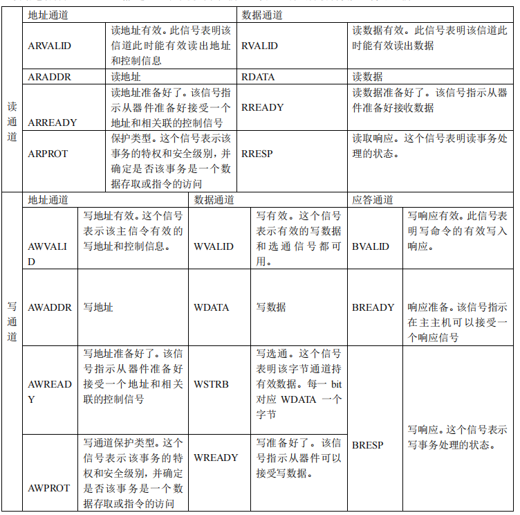
- Read address channel, including arvalid, araddr and arready signals;
- Read data channel, including rvalid, rdata, rready and rresp signals;
- Write address channel, including AWVALID, awaddr and awready signals;
- Write data channel, including WVALID, WDATA, WSTRB, WREADY signals;
- Write response channel, including bvalid, bresp and ready signals;
- System channel, including ACLK and ARESETN signals.
The signals of AXI4 bus and AXI4 Lite bus also have its naming characteristics
- All read address signals begin with AR (A: address; R: read)
- Write address signals start with AW (A: address; W: write)
- All read data signals begin with R (R: read)
- All write data signals begin with w (W: write)
- Answer models start with B (B: back (answer back))
3. Overview of Axi interface
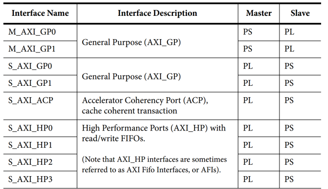
The three AXI interfaces are:
- AXI-GP interface (4): it is a general AXI interface, including two 32-bit master device interfaces and two 32-bit slave device interfaces. This interface is used
You can access the on-chip and off-chip devices in the PS. - AXI-HP interface (4): it is a standard interface with high performance / bandwidth, and the PL module is connected as the main device (as can be seen from the arrow in the figure below). main
To use PL to access memory on PS (DDR and on chip RAM) - AXI-ACP interface (1): it is an interface defined under ARM multi-core architecture. It is translated into accelerator consistency port in Chinese to manage DMA
For AXI peripherals without cache, the PS side is the Slave interface.
We can double-click to view the internal configuration of the IP core of ZYNQ, and we can find the above three interfaces, which have been marked with red boxes in the figure.
4. Overview of Axi protocol
The two ends of AXI bus protocol can be divided into master and slave. They generally need to be connected through an AXI Interconnect to provide a switching mechanism to connect one or more AXI master devices to one or more AXI slave devices.
The main function of AXI Interconnect is to connect and manage multiple hosts and slave machines. Because AXI supports out of order transmission, out of order transmission requires the support of host ID signals, and different hosts may send the same ID. AXI Interconnect solves this problem. It will process the ID signals of different hosts to make the ID unique. AXI protocol separates read address channel, read data channel, write address channel, write data channel and write response channel. Each channel has its own handshake protocol. Each channel does not interfere with each other but depends on each other. This is one of the reasons why AXI is efficient.
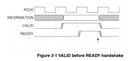
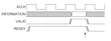
4.1 AXI protocol - handshake protocol
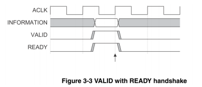
AXI4 adopts a READY and VALID handshake communication mechanism. In short, there is a handshake process before the master and slave sides conduct data communication. The transmission source generates VLAID signals to indicate when data or control information is VALID. The destination source generates a READY signal to indicate that it is READY to receive data or control information. Transmission occurs when the VALID and READY signals are both high. There are three relationships between VALID and READY signals.
2, Axi4 Lite source code learning
1. Customize AXI IP core
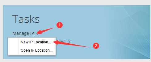
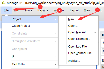
Step 1: open Vivado software - > select Manage IP - > select New IP Location
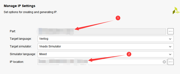
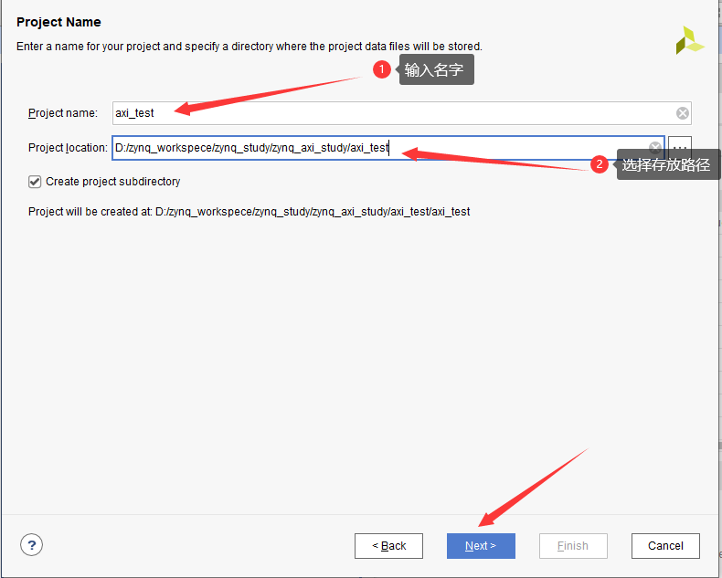
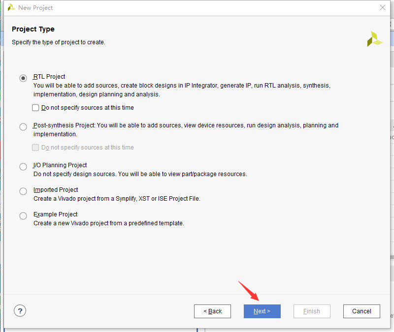
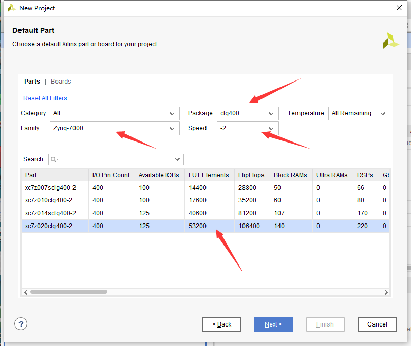
Step 2: next - > select the corresponding chip of ZYNQ at ① - > select the IP storage location at ② - > finish
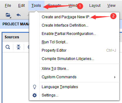
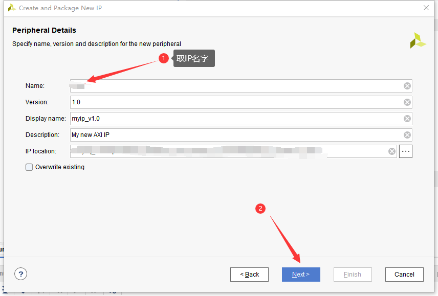
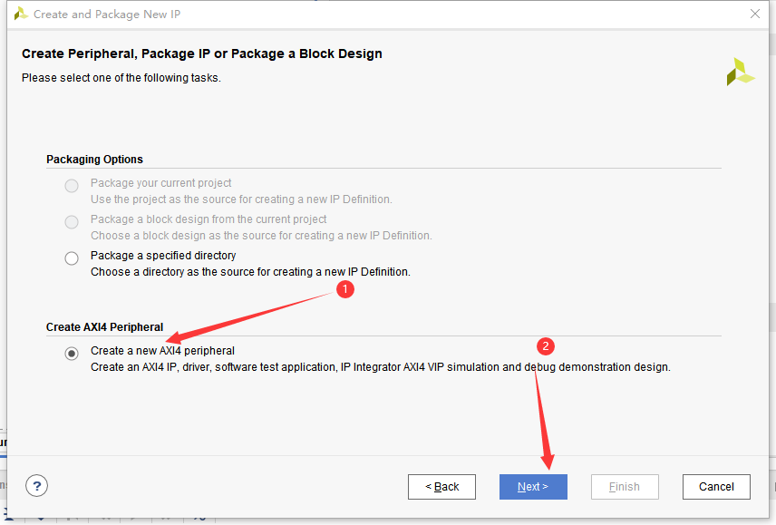
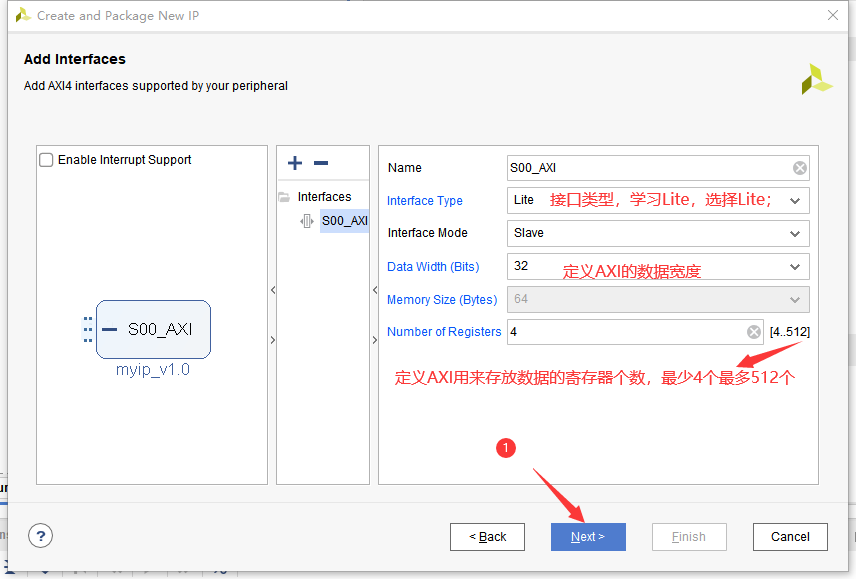
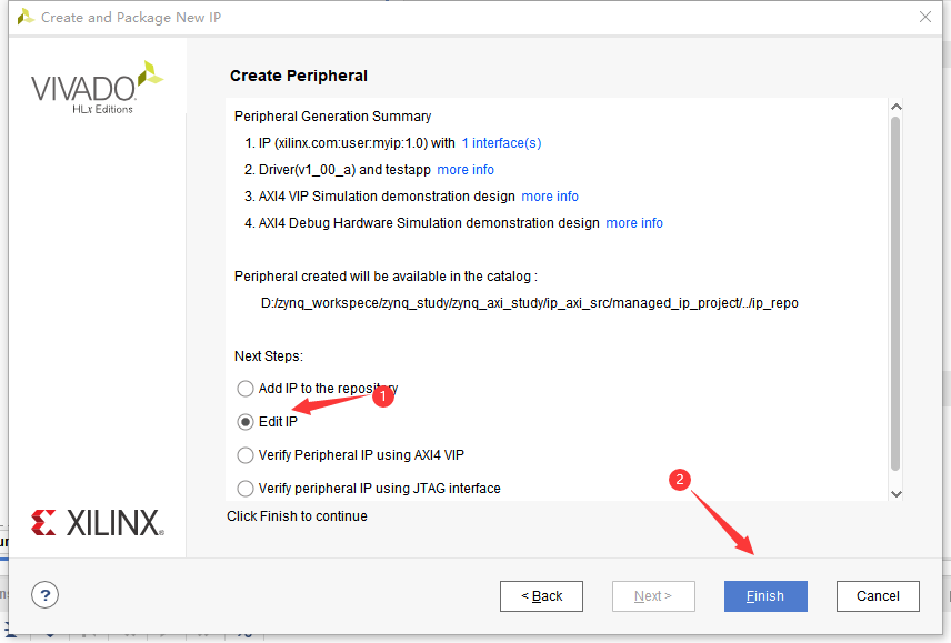
Step 3: Tools - > create and package new IP - > next - > create a new axi4 peripheral - > next - > name at ① in Figure 3 - > next - > configure IP core, as shown in Figure 4 - > next - > Edit IP - > finish
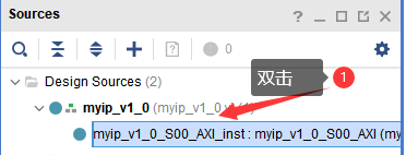
Step4: double click, as shown in Figure 1 below
2. Analysis of source code
1. First, some IP interfaces; See the table below for specific functions
		// Global Clock Signal
		input wire  S_AXI_ACLK,
		// Global Reset Signal. This Signal is Active LOW
		input wire  S_AXI_ARESETN,
		// Write address (issued by master, acceped by Slave)
		input wire [C_S_AXI_ADDR_WIDTH-1 : 0] S_AXI_AWADDR,
		// Write channel Protection type. This signal indicates the
    		// privilege and security level of the transaction, and whether
    		// the transaction is a data access or an instruction access.
		input wire [2 : 0] S_AXI_AWPROT,
		// Write address valid. This signal indicates that the master signaling
    		// valid write address and control information.
		input wire  S_AXI_AWVALID,
		// Write address ready. This signal indicates that the slave is ready
    		// to accept an address and associated control signals.
		output wire  S_AXI_AWREADY,
		// Write data (issued by master, acceped by Slave)
		input wire [C_S_AXI_DATA_WIDTH-1 : 0] S_AXI_WDATA,
		// Write strobes. This signal indicates which byte lanes hold
    		// valid data. There is one write strobe bit for each eight
    		// bits of the write data bus.
		input wire [(C_S_AXI_DATA_WIDTH/8)-1 : 0] S_AXI_WSTRB,
		// Write valid. This signal indicates that valid write
    		// data and strobes are available.
		input wire  S_AXI_WVALID,
		// Write ready. This signal indicates that the slave
    		// can accept the write data.
		output wire  S_AXI_WREADY,
		// Write response. This signal indicates the status
    		// of the write transaction.
		output wire [1 : 0] S_AXI_BRESP,
		// Write response valid. This signal indicates that the channel
    		// is signaling a valid write response.
		output wire  S_AXI_BVALID,
		// Response ready. This signal indicates that the master
    		// can accept a write response.
		input wire  S_AXI_BREADY,
		// Read address (issued by master, acceped by Slave)
		input wire [C_S_AXI_ADDR_WIDTH-1 : 0] S_AXI_ARADDR,
		// Protection type. This signal indicates the privilege
    		// and security level of the transaction, and whether the
    		// transaction is a data access or an instruction access.
		input wire [2 : 0] S_AXI_ARPROT,
		// Read address valid. This signal indicates that the channel
    		// is signaling valid read address and control information.
		input wire  S_AXI_ARVALID,
		// Read address ready. This signal indicates that the slave is
    		// ready to accept an address and associated control signals.
		output wire  S_AXI_ARREADY,
		// Read data (issued by slave)
		output wire [C_S_AXI_DATA_WIDTH-1 : 0] S_AXI_RDATA,
		// Read response. This signal indicates the status of the
    		// read transfer.
		output wire [1 : 0] S_AXI_RRESP,
		// Read valid. This signal indicates that the channel is
    		// signaling the required read data.
		output wire  S_AXI_RVALID,
		// Read ready. This signal indicates that the master can
    		// accept the read data and response information.
		input wire  S_AXI_RREADY
2. Write data related source code
always @( posedge S_AXI_ACLK )
	begin
	  if ( S_AXI_ARESETN == 1'b0 )
	    begin
	      slv_reg0 <= 0;
	      slv_reg1 <= 0;
	      slv_reg2 <= 0;
	      slv_reg3 <= 0;
	    end
	  else begin
	    if (slv_reg_wren)
	      begin
	        case ( axi_awaddr[ADDR_LSB+OPT_MEM_ADDR_BITS:ADDR_LSB] )
	          2'h0:
	            for ( byte_index = 0; byte_index <= (C_S_AXI_DATA_WIDTH/8)-1; byte_index = byte_index+1 )
	              if ( S_AXI_WSTRB[byte_index] == 1 ) begin
	                // Respective byte enables are asserted as per write strobes
	                // Slave register 0
	                slv_reg0[(byte_index*8) +: 8] <= S_AXI_WDATA[(byte_index*8) +: 8];
	              end
	          2'h1:
	            for ( byte_index = 0; byte_index <= (C_S_AXI_DATA_WIDTH/8)-1; byte_index = byte_index+1 )
	              if ( S_AXI_WSTRB[byte_index] == 1 ) begin
	                // Respective byte enables are asserted as per write strobes
	                // Slave register 1
	                slv_reg1[(byte_index*8) +: 8] <= S_AXI_WDATA[(byte_index*8) +: 8];
	              end
	          2'h2:
	            for ( byte_index = 0; byte_index <= (C_S_AXI_DATA_WIDTH/8)-1; byte_index = byte_index+1 )
	              if ( S_AXI_WSTRB[byte_index] == 1 ) begin
	                // Respective byte enables are asserted as per write strobes
	                // Slave register 2
	                slv_reg2[(byte_index*8) +: 8] <= S_AXI_WDATA[(byte_index*8) +: 8];
	              end
	          2'h3:
	            for ( byte_index = 0; byte_index <= (C_S_AXI_DATA_WIDTH/8)-1; byte_index = byte_index+1 )
	              if ( S_AXI_WSTRB[byte_index] == 1 ) begin
	                // Respective byte enables are asserted as per write strobes
	                // Slave register 3
	                slv_reg3[(byte_index*8) +: 8] <= S_AXI_WDATA[(byte_index*8) +: 8];
	              end
	          default : begin
	                      slv_reg0 <= slv_reg0;
	                      slv_reg1 <= slv_reg1;
	                      slv_reg2 <= slv_reg2;
	                      slv_reg3 <= slv_reg3;
	                    end
	        endcase
	      end
	  end
	end
When the PS writes data to the axi4 Lite bus, it stores the data transmitted from the bus in the register slv_reg. And slv_reg register has 0 ~ 3
4 in total. As for which is assigned by
axi_awaddr[ADDR_LSB+OPT_MEM_ADDR_BITS:ADDR_LSB] is determined by Axi according to the macro definition_ Awaddr [3:2] (write)
The address contains not only the address, but also the control bit. Here [3:2] is the control bit) to determine which SLV to assign_ reg.
When PS calls the write function, if the address offset is not done, Axi_ The default value of awaddr [3:2] is 0. For example, if the address of our custom IP is mapped to 0x43c00000, we__ Xil_Out32(0x43C00000,Value)__ It's SLV_ The value of reg0. If the address is offset by 4 bits, such as_ Xil_Out32(0x43C00000 + 4,Value) writes SLV_ The value of reg1, and so on;
In slv_reg0 as an example:
for ( byte_index = 0; byte_index <= (C_S_AXI_DATA_WIDTH/8)-1; byte_index = byte_index+1 )
	              if ( S_AXI_WSTRB[byte_index] == 1 ) begin
	                // Respective byte enables are asserted as per write strobes
	                // Slave register 0
	                slv_reg0[(byte_index*8) +: 8] <= S_AXI_WDATA[(byte_index*8) +: 8];
	              end
The most critical sentence in the for loop:
slv_reg0[(byte_index*8) +: 8] <= S_AXI_WDATA[(byte_index*8) +: 8];
When byte_ When index = 0, this sentence is equivalent to:
slv_reg0[7:0] <= S_AXI_WDATA[7:0];
When byte_ When index = 1, this sentence is equivalent to:
slv_reg0[15:8] <= S_AXI_WDATA[15:8];
When byte_ When index = 2, this sentence is equivalent to:
slv_reg0[23:16] <= S_AXI_WDATA[23:16];
When byte_ When index = 3, this sentence is equivalent to:
slv_reg0[31:24] <= S_AXI_WDATA[31:24];
That is, only when the write strobe signal is 1, it corresponds to S_AXI_WDATA bytes will be read.
3. Read source code analysis
// Output register or memory read data
	always @( posedge S_AXI_ACLK )
	begin
	  if ( S_AXI_ARESETN == 1'b0 )
	    begin
	      axi_rdata  <= 0;
	    end
	  else
	    begin
	      // When there is a valid read address (S_AXI_ARVALID) with
	      // acceptance of read address by the slave (axi_arready),
	      // output the read dada
	      if (slv_reg_rden)
	        begin
	          axi_rdata <= reg_data_out;     // register read data
	        end
	    end
	end
The observation shows that when PS reads data, the program will send reg_data_out copy to axi_rdata (RADTA read data). We keep tracking reg_data_out:
always @(*)
begin
 // Address decoding for reading registers
 case ( axi_araddr[ADDR_LSB+OPT_MEM_ADDR_BITS:ADDR_LSB] )
 	2'h0 : reg_data_out <= slv_reg0;
 	2'h1 : reg_data_out <= slv_reg1;
 	2'h2 : reg_data_out <= slv_reg2;
 	2'h3 : reg_data_out <= slv_reg3;
 default : reg_data_out <= 0;
 endcase
end
This program is an example provided by Vivado. It just wants to verify that the value written out is equal to the value read in.
3. Summary
If we want to use the PS side to read the Axi_ When using lite4 bus data, you can write your own code:
reg [11:0]axi_urdata;
 always @( posedge S_AXI_ACLK )
 begin
 if ( S_AXI_ARESETN == 1'b0 )
 	begin
 		axi_urdata<= 12'd0; //Reset register
	end
 else
 	begin
 		axi_urdata<= slv_reg0[11:0];//Copy the data of register 0 to the custom register
 	end
 end
 assign axi_rdata= axi_urdata;// Read data output;
If we want to pair Axi with PS side_ When writing data on lite4 bus, you can write a code yourself:
wire[31:0]axi_wdata;
always @(*)
 begin
	 case ( axi_araddr[ADDR_LSB+OPT_MEM_ADDR_BITS:ADDR_LSB] )
 		2'h0 : reg_data_out <= axi_wdata;//slv_reg0;
	 	2'h1 : reg_data_out <= slv_reg1;
 		2'h2 : reg_data_out <= slv_reg2;
 		2'h3 : reg_data_out <= slv_reg3;
 	default : reg_data_out <= 0;
 endcase
 end
3, Source code test
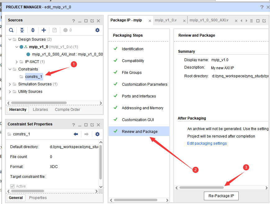
1. Encapsulate IP core
2. Create project
Step 1: create project - > next
Step2
Step3
Create an empty design
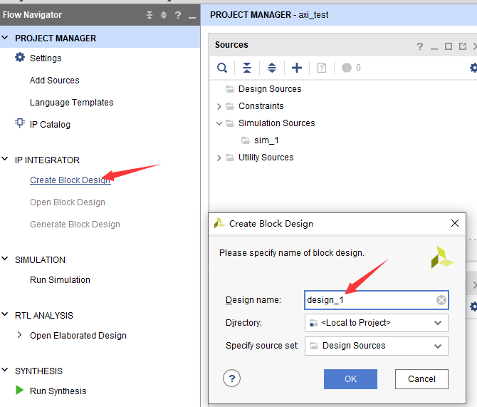
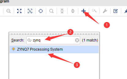
Join the IP core of ZYNQ
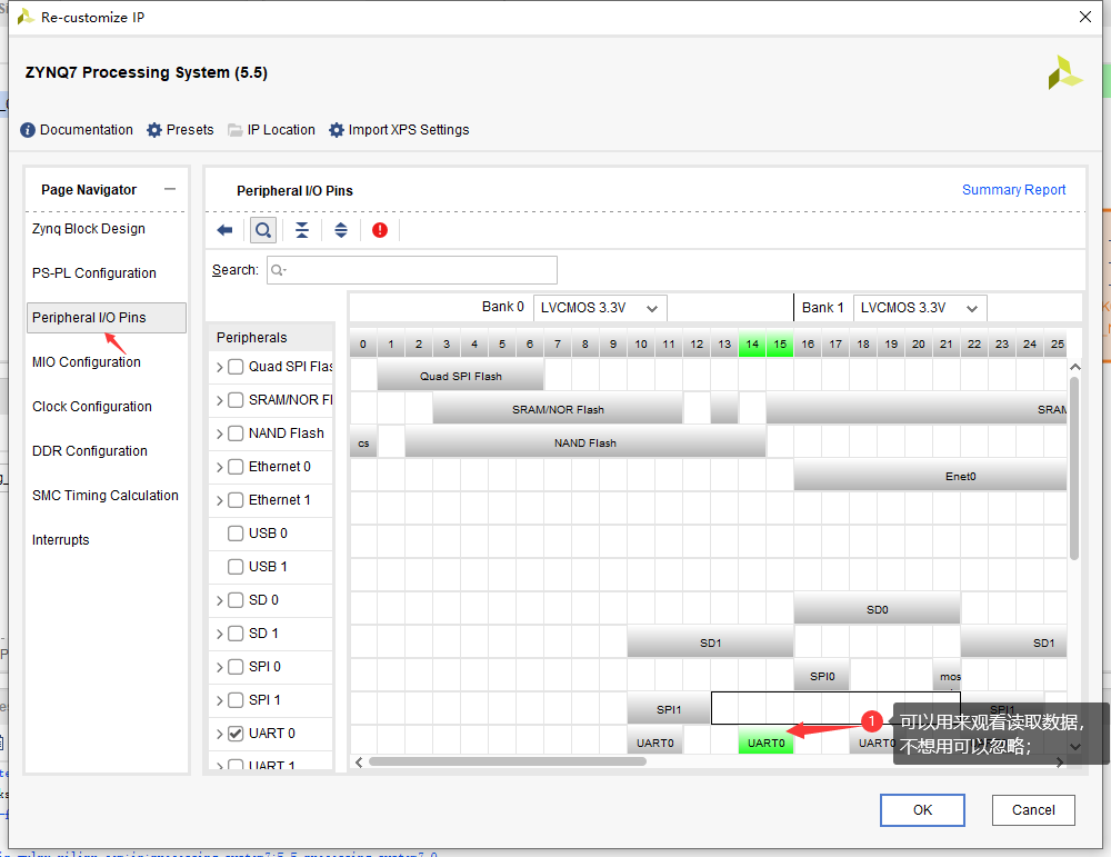
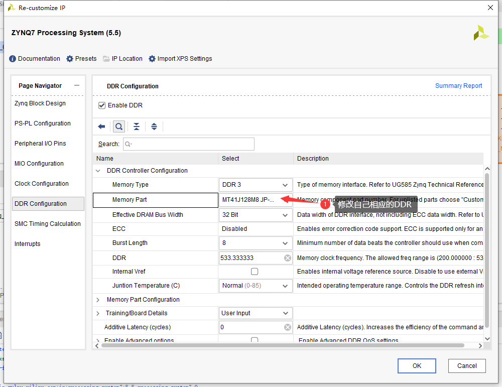
Double click ZYNQ IP to modify the corresponding configuration
Add custom IP core path
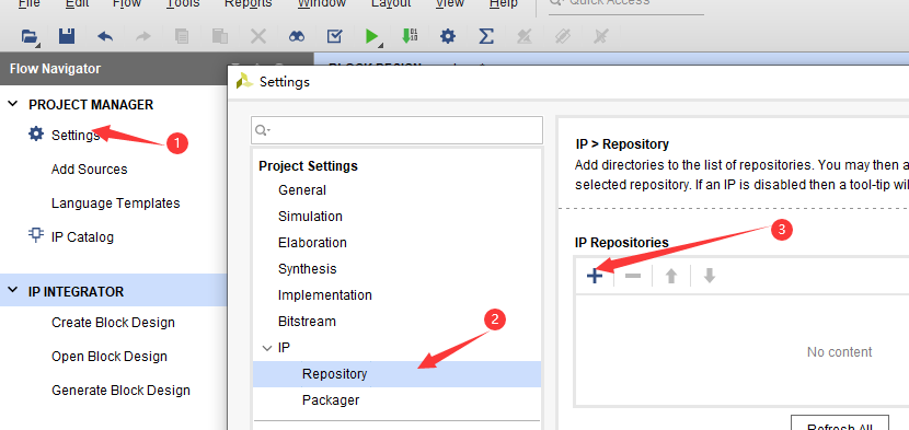
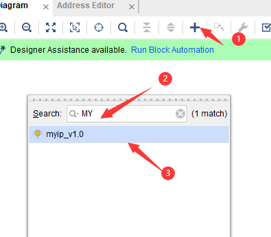
Add custom IP core
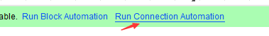
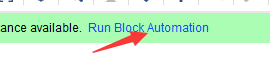
Connect automatically
Right click and click generate layout to optimize routing
Automatic deployment, connection DDR, etc
Ctrl + S what it looks like after saving
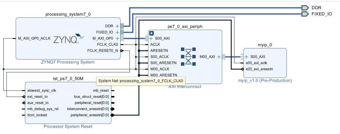
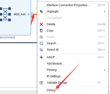
To verify whether there are errors, click the following figure;

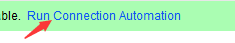
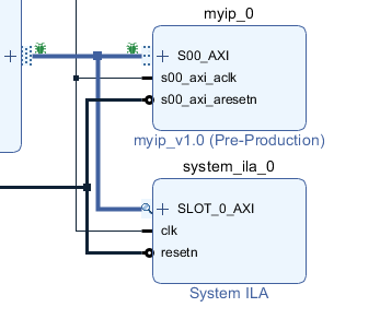
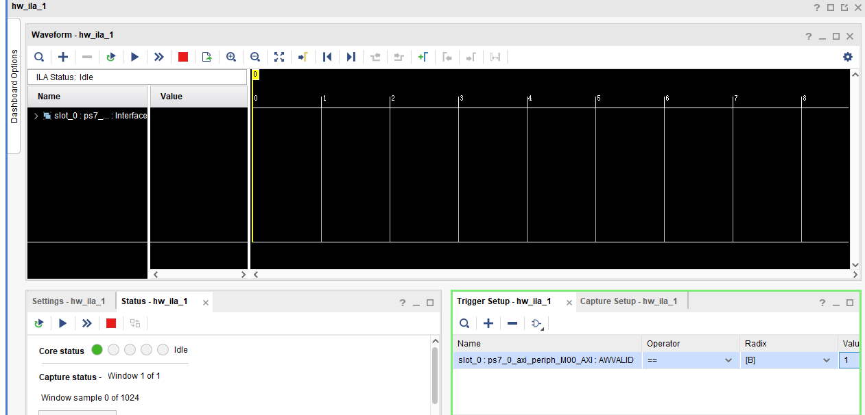
Add observation signal
How the connection looks
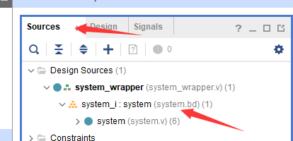
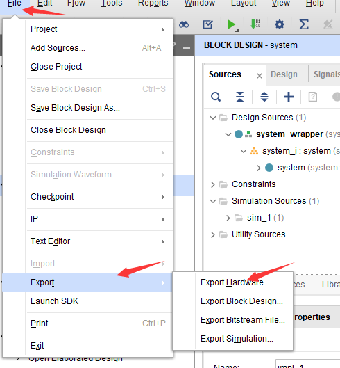
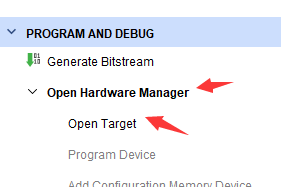
Generate hardware
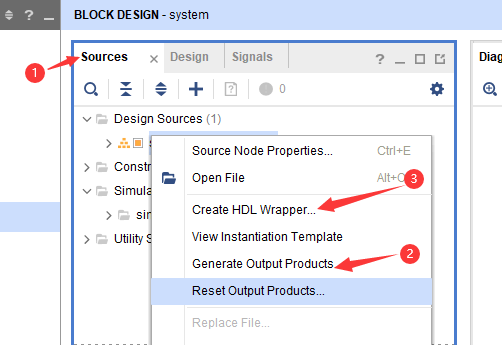
What it looks like when it's finished
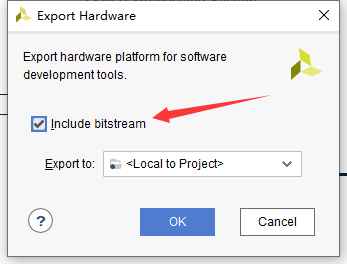
Generate bitstream
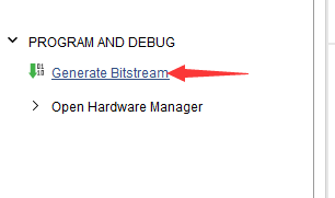
Wait for completion


3. Import SDK
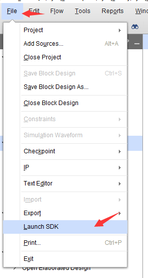
New project file - > New - > Application Project
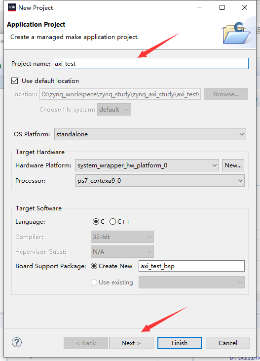
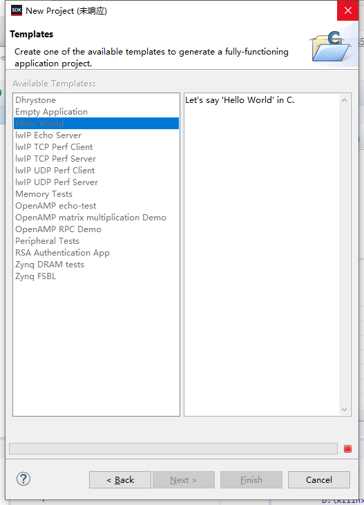
New Hello World Project
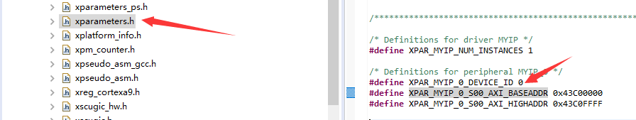
Base address found
Write data
#include <stdio.h>
#include "platform.h"
#include "xil_printf.h"
#include "xil_io.h"
#include "xil_types.h"
#include "xparameters.h"
int main()
{
volatile u32 rdata_0;
volatile u32 rdata_1;
volatile u32 rdata_2;
volatile u32 rdata_3;
while(1)
{
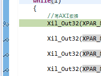
//Write AXI data
Xil_Out32(XPAR_MYIP_0_S00_AXI_BASEADDR,0x01);
Xil_Out32(XPAR_MYIP_0_S00_AXI_BASEADDR+4,0x02);
Xil_Out32(XPAR_MYIP_0_S00_AXI_BASEADDR+8,0x03);
Xil_Out32(XPAR_MYIP_0_S00_AXI_BASEADDR+12,0x04);
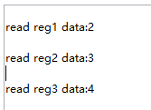
//Reading AXI data
rdata_0 = Xil_In32(XPAR_MYIP_0_S00_AXI_BASEADDR);
printf("read reg0 data:%ld\n\r",rdata_0);
rdata_1 = Xil_In32(XPAR_MYIP_0_S00_AXI_BASEADDR+4);
printf("read reg1 data:%ld\n\r",rdata_1);
rdata_2 = Xil_In32(XPAR_MYIP_0_S00_AXI_BASEADDR+8);
printf("read reg2 data:%ld\n\r",rdata_2);
rdata_3 = Xil_In32(XPAR_MYIP_0_S00_AXI_BASEADDR+12);
printf("read reg3 data:%ld\n\r",rdata_3);
}
// init_platform();
// print("Hello World\n\r");
// cleanup_platform();
// return 0;
}
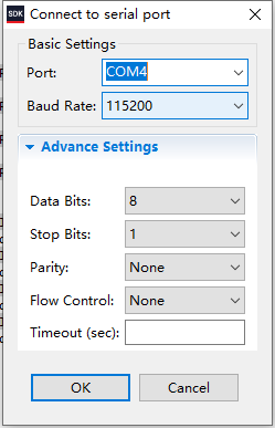
Add serial port
debugging
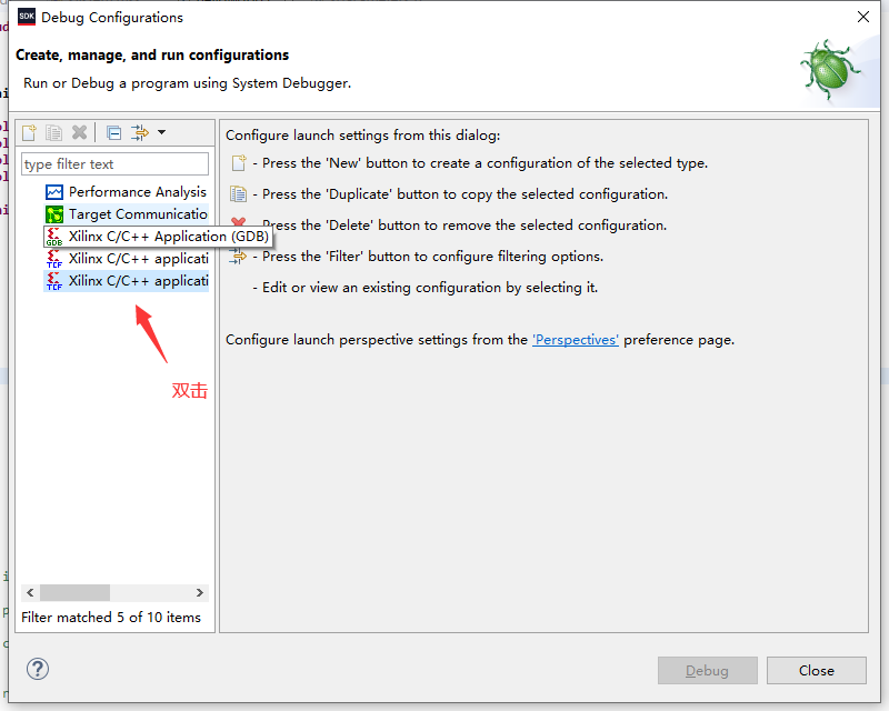
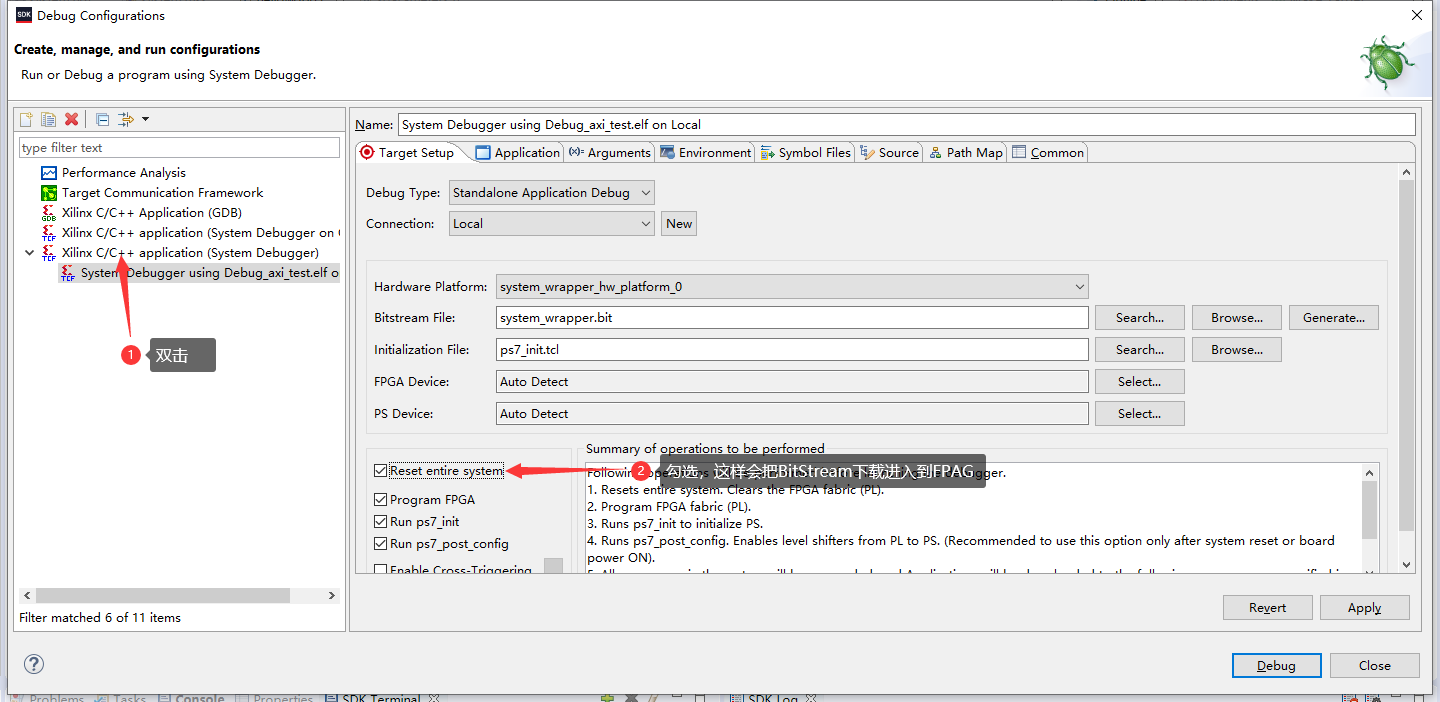
Project - > right click - > debug as - > debug configurations
Double click to set breakpoint
Generation simulation
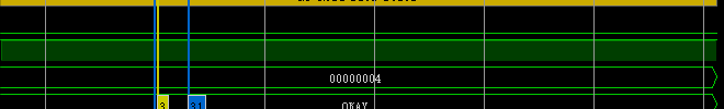
Test chart
Serial port reading diagram
Simulation diagram
4, Summary
Through this, I learned the theoretical knowledge of AXI, the internal source code of AXI, the basic steps of Vivado to establish a project, and how to create a project in the SDK and write my own application; The basic timing of AXI is tested. The AXI is written into the data through the serial port and connected with the read-out data. How to control the write and read-out of AXI bus through PS terminal is verified;
Problems: 1. The logic of key statements in source Verilog; 2. Use Verilog to write and read AXI;