Abstract: in fact, in the design of a CPU, each sub module is relatively basic and simple, but the combined overall architecture will be more complex, whether it is timing path, data path and control path. Here, we mainly introduce the sub modules of the whole microarchitecture in detail.
1. PC fetch, PC branch, instruction jump and L2 stack
PC fetch means that the PC value is mainly used as the address to read the instruction data in the program memory (EPROM) and send it to the instruction register IR. Usually, it is read out one by one, that is, the PC value is automatically increased by one in the next clock (pipelined clock) to read the instruction where the next address is located (of course, the modification of PC depends on the instruction word length and addressing mode). However, sometimes there are program branches, program jumps and so on, so that the program needs to execute the instructions of another region, so there is a PC branch.
1.1 PC branches are generally divided into the following situations:
- RETLW: return to assign stack stack1 or stack2 to PC;
- CALL: CALL, assign status[6:5],1'b0,inst[7:0] to PC;
- GOTO: jump, assign status[6:5],inst[8:0] to PC;
- MOVWF: MOVWF PCL, assign pc[10:8],dbus to PC; (in addition, there are ADDWF and BSF, which are not implemented here);
- DEFAULT: PC <- PC + 1.
1.2 for instruction Jump, the instructions that can make the instruction Jump include GOTO, CALL, RETLW, BTFSC, BTFSS, DECFSZ and INCFSZ.
1.3. For the call and return of stacklevel, the state machine is used, as follows. The number in the circle represents stack level, and the number on the right represents the number of subroutine layers that have been called.
-
When the CALL instruction is executed, the stack pressing operation is push ed, the PC assigns a value to the stack, and changes the state of stacklevel at the same time;
-
When RETLW instruction is executed, pop-up operation pop is performed, the stack is returned to PC, and the state of stacklevel is changed at the same time.
The detailed circuit module and Verilog code are as follows:
always @(posedge clk) begin
   if (!rst_n)
      pc <= RESET_VECTOR;
   else
      pc <= pc_mux;
end

always @(inst or stacklevel or status or stack1 or stack2 or pc or dbus) begin
   casex ({inst, stacklevel})
      14'b1000_????_????_11: pc_mux = stack2;           // RETLW
      14'b1000_????_????_01: pc_mux = stack1;           // RETLW
      14'b1001_????_????_??: pc_mux = {status[6:5], 1'b0, inst[7:0]}; // CALL
      14'b101?_????_????_??: pc_mux = {status[6:5],       inst[8:0]}; // GOTO
      14'b00?0_0010_0010_??: pc_mux = {pc[10:8], dbus}; // MOVWF PCL
      default:
         pc_mux = pc + 11'd1;
   endcase
end

always @(posedge clk) begin
   if (!rst_n) begin
      stack1 <= 11'd0;
      stack2 <= 11'd0;
   end
   else begin
      // CALL Instruction
      if (inst[11:8] == 4'b1001) begin
         case (stacklevel)
            2'b00: stack1 <= pc;
            2'b01: stack2 <= pc;
          default: begin
                   stack1 <= 11'd0;
                   stack2 <= 11'd0;
                   end
         endcase
      end
   end
end

always @(posedge clk) begin
   if (!rst_n)
      stacklevel <= 2'b00;
   else begin
      casex ({inst, stacklevel})
         // CALL Instruction
         14'b1001_????_????_00: stacklevel <= 2'b01;  // Record 1st CALL
         14'b1001_????_????_01: stacklevel <= 2'b11;  // Record 2nd CALL
         14'b1001_????_????_11: stacklevel <= 2'b11;  // Ignore
         // RETLW Instruction
         14'b1000_????_????_11: stacklevel <= 2'b01;  // Go back to 1 CALL in progress
         14'b1000_????_????_01: stacklevel <= 2'b00;  // Go back to no CALL in progress
         14'b1000_????_????_00: stacklevel <= 2'b00;  // Ignore
         default:
            stacklevel <= stacklevel;
      endcase
   end
end

always @(posedge clk) begin
   if(!rst_n)
      inst <= 12'h000;
   else begin
      if(skip == 1'b1)
         inst <= 12'b000000000000; // FORCE NOP
      else
         inst <= inst_data;
   end
end

always @(inst or aluz) begin
   casex ({inst, aluz})
      13'b10??_????_????_?: skip = 1'b1; // A GOTO, CALL or RETLW instructions
      13'b0110_????_????_1: skip = 1'b1; // BTFSC instruction  and aluz == 1
      13'b0111_????_????_0: skip = 1'b1; // BTFSS instruction  and aluz == 0
      13'b0010_11??_????_1: skip = 1'b1; // DECFSZ instruction and aluz == 1
      13'b0011_11??_????_1: skip = 1'b1; // INCFSZ instruction and aluz == 1
                   default: skip = 1'b0;
   endcase
end
2. Instruction decoding
The instruction decoding is mainly realized through the combinational logic hardware circuit (in the form of Look Up Table), and the key control and status signals are provided for the instruction. For the specific decoding method, refer to the following code.
aluasel, alubsel: it is mainly used to select the operands of ALU module. The operands generally come from W register, F file register and instruction immediate;
aluop: it is mainly used to select the operation of ALU module, such as addition, subtraction, and, or, non, XOR, shift left, shift right and half byte exchange;
wwe, fwe: mainly write enable of W and F registers;
zwe, cwe: mainly write enable the Z and C STATUS bits of the STATUS register;
bdpol: related to bit oriented operation instructions;
tris: control I/O input and output status (none);
OPTION: OPTION register (none).
The detailed circuit module and Verilog code are as follows:
module IDec (
	inst,
	aluasel,
	alubsel,
	aluop,
	wwe,
	fwe,
	zwe,
	cwe,
	bdpol,
	option,
	tris
);

input  [11:0]	inst;
output [1:0]	aluasel;
output [1:0]	alubsel;
output [3:0]	aluop;
output			wwe;
output			fwe;
output			zwe;
output			cwe;
output			bdpol;
output			option;
output			tris;

reg [14:0] decodes;

assign {aluasel,	// Select source for ALU A input. 00=W, 01=SBUS, 10=K, 11=BD
		alubsel,	// Select source for ALU B input. 00=W, 01=SBUS, 10=K, 11="1"
		aluop,		// ALU Operation (see comments above for these codes)
		wwe,		// W register Write Enable
		fwe,		// File Register Write Enable
		zwe,		// Status register Z bit update
		cwe,		// Status register Z bit update
		bdpol,		// Polarity on bit decode vector (0=no inversion, 1=invert)
		tris,		// Instruction is an TRIS instruction
		option		// Instruction is an OPTION instruction
	} = decodes;

always @(inst) begin
	casex (inst)
		// *** Byte-Oriented File Register Operations
		//
		//                                 A  A  ALU  W F Z C B T O
		//                                 L  L   O   W W W W D R P
		//                                 U  U   P   E E E E P I T
		//                                 A  B               O S
		//                                                    L
		12'b0000_0000_0000: decodes = 15'b00_00_0000_0_0_0_0_0_0_0; // NOP
		12'b0000_001X_XXXX: decodes = 15'b00_00_0010_0_1_0_0_0_0_0; // MOVWF
		12'b0000_0100_0000: decodes = 15'b00_00_0011_1_0_1_0_0_0_0; // CLRW
		12'b0000_011X_XXXX: decodes = 15'b00_00_0011_0_1_1_0_0_0_0; // CLRF
		12'b0000_100X_XXXX: decodes = 15'b01_00_1000_1_0_1_1_0_0_0; // SUBWF (d=0)
		12'b0000_101X_XXXX: decodes = 15'b01_00_1000_0_1_1_1_0_0_0; // SUBWF (d=1)
		12'b0000_110X_XXXX: decodes = 15'b01_11_1000_1_0_1_0_0_0_0; // DECF  (d=0)
		12'b0000_111X_XXXX: decodes = 15'b01_11_1000_0_1_1_0_0_0_0; // DECF  (d=1)
		12'b0001_000X_XXXX: decodes = 15'b00_01_0010_1_0_1_0_0_0_0; // IORWF (d=0)
		12'b0001_001X_XXXX: decodes = 15'b00_01_0010_0_1_1_0_0_0_0; // IORWF (d=1)
		12'b0001_010X_XXXX: decodes = 15'b00_01_0001_1_0_1_0_0_0_0; // ANDWF (d=0)
		12'b0001_011X_XXXX: decodes = 15'b00_01_0001_0_1_1_0_0_0_0; // ANDWF (d=1)
		12'b0001_100X_XXXX: decodes = 15'b00_01_0011_1_0_1_0_0_0_0; // XORWF (d=0)
		12'b0001_101X_XXXX: decodes = 15'b00_01_0011_0_1_1_0_0_0_0; // XORWF (d=1)
		12'b0001_110X_XXXX: decodes = 15'b00_01_0000_1_0_1_1_0_0_0; // ADDWF (d=0)
		12'b0001_111X_XXXX: decodes = 15'b00_01_0000_0_1_1_1_0_0_0; // ADDWF (d=1)
		12'b0010_000X_XXXX: decodes = 15'b01_01_0010_1_0_1_0_0_0_0; // MOVF  (d=0)
		12'b0010_001X_XXXX: decodes = 15'b01_01_0010_0_1_1_0_0_0_0; // MOVF  (d=1)
		12'b0010_010X_XXXX: decodes = 15'b01_01_0100_1_0_1_0_0_0_0; // COMF  (d=0)
		12'b0010_011X_XXXX: decodes = 15'b01_01_0100_0_1_1_0_0_0_0; // COMF  (d=1)
		12'b0010_100X_XXXX: decodes = 15'b01_11_0000_1_0_1_0_0_0_0; // INCF  (d=0)
		12'b0010_101X_XXXX: decodes = 15'b01_11_0000_0_1_1_0_0_0_0; // INCF  (d=1)
		12'b0010_110X_XXXX: decodes = 15'b01_11_1000_1_0_0_0_0_0_0; // DECFSZ(d=0)
		12'b0010_111X_XXXX: decodes = 15'b01_11_1000_0_1_0_0_0_0_0; // DECFSZ(d=1)
		12'b0011_000X_XXXX: decodes = 15'b01_01_0101_1_0_0_1_0_0_0; // RRF   (d=0)
		12'b0011_001X_XXXX: decodes = 15'b01_01_0101_0_1_0_1_0_0_0; // RRF   (d=1)
		12'b0011_010X_XXXX: decodes = 15'b01_01_0110_1_0_0_1_0_0_0; // RLF   (d=0)
		12'b0011_011X_XXXX: decodes = 15'b01_01_0110_0_1_0_1_0_0_0; // RLF   (d=1)
		12'b0011_100X_XXXX: decodes = 15'b01_01_0111_1_0_0_0_0_0_0; // SWAPF (d=0)
		12'b0011_101X_XXXX: decodes = 15'b01_01_0111_0_1_0_0_0_0_0; // SWAPF (d=1)
		12'b0011_110X_XXXX: decodes = 15'b01_11_0000_1_0_0_0_0_0_0; // INCFSZ(d=0)
		12'b0011_111X_XXXX: decodes = 15'b01_11_0000_0_1_0_0_0_0_0; // INCFSZ(d=1)

		// *** Bit-Oriented File Register Operations
		12'b0100_XXXX_XXXX: decodes = 15'b11_01_0001_0_1_0_0_1_0_0; // BCF
		12'b0101_XXXX_XXXX: decodes = 15'b11_01_0010_0_1_0_0_0_0_0; // BSF
		12'b0110_XXXX_XXXX: decodes = 15'b11_01_0001_0_0_0_0_0_0_0; // BTFSC
		12'b0111_XXXX_XXXX: decodes = 15'b11_01_0001_0_0_0_0_0_0_0; // BTFSS

		// *** Literal and Control Operations
		12'b0000_0000_0010: decodes = 15'b00_00_0010_0_1_0_0_0_0_1; // OPTION
		12'b0000_0000_0011: decodes = 15'b00_00_0000_0_0_0_0_0_0_0; // SLEEP
		12'b0000_0000_0100: decodes = 15'b00_00_0000_0_0_0_0_0_0_0; // CLRWDT
		12'b0000_0000_0101: decodes = 15'b00_00_0010_0_1_0_0_0_1_0; // TRIS 5
		12'b0000_0000_0110: decodes = 15'b00_00_0010_0_1_0_0_0_1_0; // TRIS 6
		12'b0000_0000_0111: decodes = 15'b00_00_0010_0_1_0_0_0_1_0; // TRIS 7

		12'b1000_XXXX_XXXX: decodes = 15'b10_10_0010_1_0_0_0_0_0_0; // RETLW
		12'b1001_XXXX_XXXX: decodes = 15'b10_10_0010_0_0_0_0_0_0_0; // CALL
		12'b101X_XXXX_XXXX: decodes = 15'b10_10_0010_0_0_0_0_0_0_0; // GOTO
		12'b1100_XXXX_XXXX: decodes = 15'b10_10_0010_1_0_0_0_0_0_0; // MOVLW
		12'b1101_XXXX_XXXX: decodes = 15'b00_10_0010_1_0_1_0_0_0_0; // IORLW
		12'b1110_XXXX_XXXX: decodes = 15'b00_10_0001_1_0_1_0_0_0_0; // ANDLW
		12'b1111_XXXX_XXXX: decodes = 15'b00_10_0011_1_0_1_0_0_0_0; // XORLW
				   default: decodes = 15'b00_00_0000_0_0_0_0_0_0_0;
	endcase
end

endmodule
3. Instruction execution
The ALU module can basically perform all instruction operations. It may not be optimal, but it is complete.
alua, alub: operands, which perform the data operation of the corresponding instruction by selecting operands, such as W register, F register sbus, constant K, bit operand bd, and constant 1;
aluop: operation code, including nine arithmetic and logic operations: addition, subtraction, and, or, non, XOR, left shift, right shift and half byte exchange;
cin: as the low order of RRF for shift right operation;
Aluout: the operation result is output to the data bus as the output of ALU module, and finally select whether to save it in W register or F register; For example, aluout - > W or aluout - > DBUS -> regfilein --> regfileout ...> sbus;
zout, cout: flag bit, the change of status bit that may be caused by ALU operation.
The detailed circuit module and Verilog code are as follows:
module ALU(
alua,
alub,
aluop,
cin,
aluout,
zout,
cout
);
input [7:0] alua;
input [7:0] alub;
input [3:0] aluop;
input cin;
output reg [7:0] aluout;
output reg zout;
output reg cout;
reg addercout;
parameter ALUOP_ADD = 4'b0000;
parameter ALUOP_SUB = 4'b1000;
parameter ALUOP_AND = 4'b0001;
parameter ALUOP_OR = 4'b0010;
parameter ALUOP_XOR = 4'b0011;
parameter ALUOP_COM = 4'b0100;
parameter ALUOP_ROR = 4'b0101;
parameter ALUOP_ROL = 4'b0110;
parameter ALUOP_SWAP = 4'b0111;
always @(alua or alub or cin or aluop) begin
case (aluop)
ALUOP_ADD: {addercout, aluout} = alua + alub;
ALUOP_SUB: {addercout, aluout} = alua - alub;
ALUOP_AND: {addercout, aluout} = {1'b0, alua & alub};
ALUOP_OR: {addercout, aluout} = {1'b0, alua | alub};
ALUOP_XOR: {addercout, aluout} = {1'b0, alua ^ alub};
ALUOP_COM: {addercout, aluout} = {1'b0, ~alua};
ALUOP_ROR: {addercout, aluout} = {alua[0], cin, alua[7:1]};
ALUOP_ROL: {addercout, aluout} = {alua[7], alua[6:0], cin};
ALUOP_SWAP: {addercout, aluout} = {1'b0, alua[3:0], alua[7:4]};
default: {addercout, aluout} = {1'b0, 8'h00};
endcase
end
always @(aluout)
zout = (aluout == 8'h00);
always @(addercout or aluop)
if(aluop == ALUOP_SUB)
cout = ~addercout;
else
cout = addercout;
endmodule
always @(aluasel or w or sbus or k or bd) begin
case (aluasel)
2'b00: alua = w;
2'b01: alua = sbus;
2'b10: alua = k;
2'b11: alua = bd;
endcase
end
always @(alubsel or w or sbus or k) begin
case (alubsel)
2'b00: alub = w;
2'b01: alub = sbus;
2'b10: alub = k;
2'b11: alub = 8'b00000001;
endcase
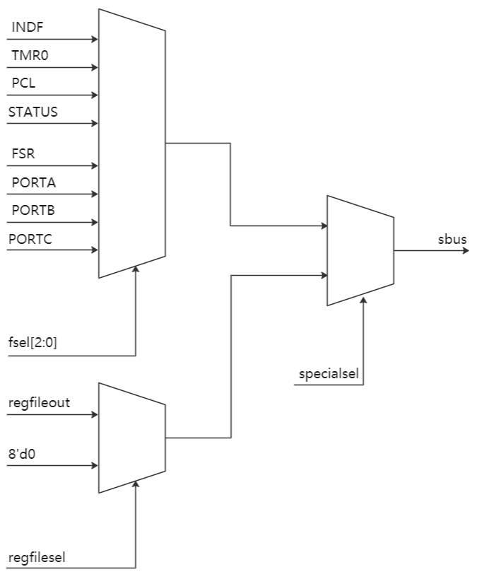
end4. Direct deposit access, indirect deposit access and relative deposit access
Direct memory access is the address of a register or memory in an instruction;
Indirect memory access is to access the register, and then there is the address of the register or memory in the register; For example, INDF Register is a global register with mappings in all banks, regardless of the setting of the Bank. It does not represent the address itself, but the unit to which the indirect address points;
Relative memory access refers to page memory access, which improves the storage capacity by expanding the page, and realizes memory access by selecting the page address (in PA1 and PA0 of STATUS) as the high bit of PC value.
Through the determination of the instruction address, the corresponding control signal is output, and the corresponding register is selected for reading and writing.
The detailed circuit module and Verilog code are as follows:
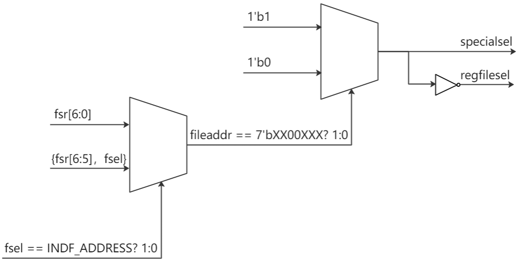
always @(fsel or fsr) begin
   if (fsel == INDF_ADDRESS)
      fileaddr = fsr[6:0]; // Indirect
   else
      fileaddr = {fsr[6:5], fsel}; // Direct
end

always @(fileaddr) begin
   casex (fileaddr)
      7'bXX00XXX: begin
            specialsel	= 1'b1;
            regfilesel	= 1'b0;
      end
      default: begin
            specialsel	= 1'b0;
            regfilesel	= 1'b1;
      end
   endcase
end

always @(*) begin
   if(specialsel) begin
      case (fsel[2:0])
         3'h0:	sbus = fsr;
         3'h1:	sbus = tmr0;
         3'h2:	sbus = pc[7:0];
         3'h3:	sbus = status;
         3'h4:	sbus = fsr;
         3'h5:	sbus = porta; // PORTA is an input-only port
         3'h6:	sbus = portb; // PORTB is an output-only port
         3'h7:	sbus = portc; // PORTC is an output-only port
      endcase
   end
   else begin
         if(regfilesel)
            sbus = regfileout;
         else
            sbus = 8'h00;
   end
end
5. F register and W register
F register is divided into special register and general register. Special register is stored as a separate register. Like W register, general register exists in the form of RAM. Their read-write delay requires a clock for writing data and no clock for reading data.
The key circuit modules and Verilog codes are as follows:
`define DEBUG_SHOWREADS
`define DEBUG_SHOWWRITES

module regs(clk, rst_n, we, re, bank, location, din, dout);

input		clk;
input		rst_n;
input		we;
input		re;
input  [1:0]	bank;
input  [4:0]	location;
input  [7:0]	din;
output [7:0]	dout;

reg [6:0]	final_address;

dram dram (
   .clk		(clk),
   .address	(final_address),
   .we		(we),
   .din		(din),
   .dout	   (dout)
);

always @(bank or location) begin
   casex ({bank, location})
      7'b00_01XXX: final_address = {4'b0000, location[2:0]};
      7'b01_01XXX: final_address = {4'b0000, location[2:0]};
      7'b10_01XXX: final_address = {4'b0000, location[2:0]};
      7'b11_01XXX: final_address = {4'b0000, location[2:0]};
      // Bank #0
      7'b00_10XXX: final_address = {4'b0001, location[2:0]};
      7'b00_11XXX: final_address = {4'b0010, location[2:0]};
      // Bank #1
      7'b01_10XXX: final_address = {4'b0011, location[2:0]};
      7'b01_11XXX: final_address = {4'b0100, location[2:0]};
      // Bank #2
      7'b10_10XXX: final_address = {4'b0101, location[2:0]};
      7'b10_11XXX: final_address = {4'b0110, location[2:0]};
      // Bank #3
      7'b11_10XXX: final_address = {4'b0111, location[2:0]};
      7'b11_11XXX: final_address = {4'b1000, location[2:0]};
      default:     final_address = {4'b0000, location[2:0]};
   endcase
end
endmodule

module dram (
   clk,
   address,
   we,
   din,
   dout
);

input		 clk;
input  [6:0] address;
input		 we;
input  [7:0] din;
output [7:0] dout;

parameter word_depth = 72;

reg [7:0] mem [0:word_depth-1];

assign dout = mem[address];

always @(posedge clk)
	if (we)
		mem[address] <= din;

endmodule
Recently, I'm busy and in a hurry. These are almost the key modules. Of course, they are storage mapping, writing of special registers, TMR0 pre frequency division, writing of test programs, etc. I haven't given the details of the whole project Download link.
I hope you can improve your FPGA design level by learning the relatively simple RISC CPU design, so the purpose of this paper has been achieved~